第3章 零件元件#
CHAPTER 3 Pieces Parts
要构建一个电路,需要各种元件,也需要很多小零件。正如我一位朋友常说的那样,你越了解这些“零件元件”的工作原理,你构建的东西就会越好。如今所有这些元件(包括最基本的三种)都有不同的封装类型,但一般分为两大类:SMT 和 TH。SMT 是表面贴装技术(Surface Mount Technology)的缩写,TH 是穿孔(Through Hole)的意思。穿孔技术是这两者中较早的一种。它易于原型制作,通常其引脚穿过 PCB(印刷电路板)上的孔。 [1] 表面贴装技术的发明主要是为了缩小尺寸,同时也加速了自动化组装。其显著特点是它直接安装在 PCB 的一个表面上。虽然形状和尺寸有所不同,但功能并未改变。当我们查看一些常见元件的图片时,请注意引脚排列和实际元件可能会有所不同。 [2]
It takes parts to make a circuit, and lots of pieces, too. The better you know how these“pieces parts” work, as a friend of mine likes to say, the better stuff you will build. These days all these parts (as well as the basic three) come in differ- ent package types but generally two categories, SMT and TH. SMT stands for surface mount technology and TH means through hole. Through hole is the older of the two types. It was and is easy to prototype with and typically has pins poking through holes in the PCB or printed circuit board. [1] Surface mount was invented to make things smaller generally speaking and also accelerated automatic assembly. Its distinguishing factor is that it mounts to the surface of one side of a PCB. While the shape and sizes change the functions do not. As we look at some pictures of typical parts please note that the pin-out and actual parts may vary. [2]
部分导电#
PARTIALLY CONDUCTING ELECTRICITY
半导体#
Semiconductors
市面上有很多教科书可以讲述半导体工作的量子力学原理。但在这里,我认为更合适的是为你提供一种关于半导体元件的基本直觉理解。
首先,什么是半导体?此处的“导体”是指电的传导。可以将半导体理解为一种部分导电的材料,或一种导电性能不完全优秀的材料。它类似于我们刚学过的电阻器, [3] 是一种可以导电但不容易导电的元件。实际上,电流越大,它对电流的阻碍越强,发热也越多。
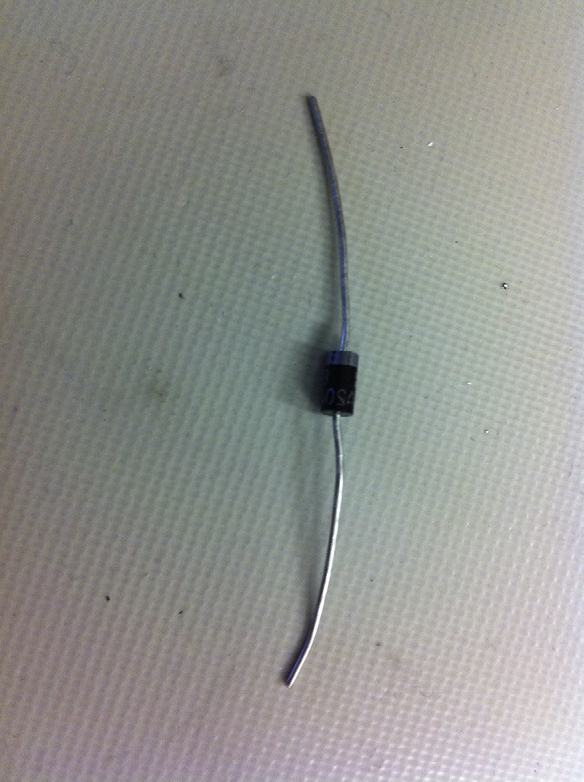
图 3.1 二极管。#
在我们继续之前,还有一个要点需要说明。半导体器件世界可以分为两大类:电流驱动型与电压驱动型。 [4] 电流驱动型元件需要电流流动才能动作。电压驱动型器件则响应输入端电压的变化。所需的电流或电压量取决于你使用的器件类型。
Texts are available that can give you the quantum mechanical principles on which a semiconductor works. However, in this context I think the better thing to do is to give you a basic intuitive understanding of semiconductor components.
First, what is a semiconductor? Conductor in this case refers to the conduction of electricity. Think of a semiconductor as a material that partially conducts elec- tricity or a material that is only semi-good at conducting electricity. It is similar to the resistor [3] that we just learned about; it’s a component that will conduct electricity but not easily. In fact, the more you push through it, the hotter it gets as it resists this flow of electricity.
FIGURE 3.1 A diode.#
Before we move on, there is one other point to make. The world of semicon- ductor devices can be grouped into two categories: current driven and voltage driven. [4] Current-driven parts require current flow to get them to act. Voltage- driven devices respond to a change in voltage at the input. How much current or voltage is needed depends on the device you are dealing with.
二极管#
Diodes
我们将从二极管开始讨论(见 Figure 3.1)。二极管是由两种类型的半导体压合而成的。它们被称为 P 型和 N 型。它们是通过一种称为掺杂(doping)的工艺制成的。在硅晶体中掺杂会引入一种杂质,从而影响晶体的结构。所引入的杂质类型可以在电子流动方面引发一些非常有趣的效果。
图 3.2 二极管的 PN 结。#
某些掺杂物会形成 N 型结构,其特点是有些额外电子“闲逛”,但没有去处。其他掺杂物会形成 P 型结构,其中存在电子缺失,称为“空穴”。于是我们得到了一个能稍微导通负电荷的 N 型材料。而另一种材料不仅不导电,反而有空穴需要填补。当我们将这两种材料压合在一起时,就会出现一种非常酷的现象;Figure 3.2 显示了这种被称为二极管的单向电子阀门。
由于空穴与自由电子的相互作用, [5] 二极管只能让电流单向流动。理想的二极管在一个方向上可以无损导电。实际中,二极管具有两个需要考虑的重要特性:正向压降与反向击穿电压——见 Figure 3.3。
图 3.3 典型二极管电压–电流响应曲线。#
We will start our discussion with the diode (see Figure 3.1). A diode is made of two types of semiconductors pushed together. They are known as type P and type N. They are created by a process called doping. In doping the silicon, an impurity is created in the crystal that affects the structure of the crystal. The type of impurity created can cause some very cool effects in silicon as it relates to electron flow.
FIGURE 3.2 The PN junction of the diode.#
Some dopants will create a type N structure in which there are some extra electrons simply hanging out with nowhere to go. Other dopants will create a type P structure in which there are missing electrons, also called holes. So we have one type N that will conduct negative charges with a little effort. We have another type that not only does not conduct but actually has holes that need filling. A cool thing happens when we smash these two types together; Figure 3.2 shows a sort of one-way electron valve known as the diode.
Due to the interaction of the holes and the free electrons, [5] a diode allows cur- rent to flow in only one direction. A perfect diode would conduct electricity in one direction without any effect on the signal. In actuality, a diode has two important characteristics to consider: the forward voltage drop and the reverse breakdown voltage—see Figure 3.3.
FIGURE 3.3 Typical diode voltage–current response.#
正向电压#
Forward Voltage
正向电压是指让电流通过二极管所需的最小电压。这一点很重要,因为如果你试图让一个电压信号通过一个低于其正向压降的二极管,你会发现它根本通不过。另一个常被忽视的事实是:正向电压乘以通过二极管的电流就是在二极管结(PN 结,即 P 和 N 材料交汇点)处所耗散的功率。如果这个功率超过了二极管的功率额定值,你很快就会看到“魔法烟”冒出来,二极管也就烧毁了。
例如,假设你有一个正向电压为 0.7 V 的二极管,而电路中电流为 2 A。那么这个二极管将以热的形式耗散 1.4 W 的能量(就像电阻器一样)。确保你选择的二极管能够承受所需功率是一个重要的经验法则。
The forward voltage is the amount of voltage needed to get current to flow across a diode. This is important to know because if you are trying to get a signal through a diode that is less than the forward voltage, you will be disappointed. Another often overlooked fact is that the forward voltage times the current through the diode is the amount of power being dissipated at the diode junction (the junction is simply the place where the P and N materials meet). If this power exceeds the wattage rat- ing of the diode, you will soon see the magic smoke come out and the diode will be toast.
For example, you have a diode with a forward-voltage rating of 0.7 V and the circuit draws 2 A. This diode will be dissipating 1.4 W of energy as heat (just like a resistor). Verifying that your selection of diode can handle the power needed is an important rule of thumb.
反向击穿电压#
Reverse Breakdown Voltage
虽然理想的二极管可以阻挡任何大小的电压,但事实是,就像人类一样,每个二极管都有其极限价格。如果反向方向的电压足够高,电流仍然会流过。这个点被称为 击穿电压 或 峰值反向电压(PIV) 。 [6] 这个电压通常很高,但请记住它是可以被达到的,特别是在你的电路中切换电感器或电动机时。
Although a perfect diode could block any amount of voltage, the fact is, just like humans, every diode has its price. If the voltage in the reverse direction gets high enough, current will flow. The point at which this happens is called the breakdown voltage or the peak inverse voltage. [6] This voltage usually is pretty high, but keep in mind that it can be reached, especially if you are switching an inductor or motor in your circuit.
晶体管#
Transistors
接下来介绍的半导体器件是在二极管结构的基础上再添加一个 P 型或 N 型结。这种器件称为 BJT,全称为双极结型晶体管,简称晶体管。在下一页有几种常见晶体管封装的图片——表面贴装和穿孔式(见 Figure 3.4)。它们有两种类型:NPN 和 PNP——见 Figure 3.5。我猜你应该能猜出这些标签的由来。
乍一看,你可能会说:“这不就是两个二极管反向串联起来吗?这不是会阻止电流向任意方向流动吗?”没错,它确实是两个二极管连接在一起,并且确实会阻止电流流动。除非你在中间部分——也就是晶体管的基极(base)——施加电流。当电流加在基极上时,该结就被激活 [7],电流便可以通过晶体管流动。晶体管的其他两个引脚称为 集电极(collector) 和 发射极(emitter)。
NPN 晶体管需要向基极注入电流才能导通,而 PNP 晶体管则需要从基极抽出电流才能导通。 [8] 换句话说,NPN 需要基极比发射极更正(更高电位),
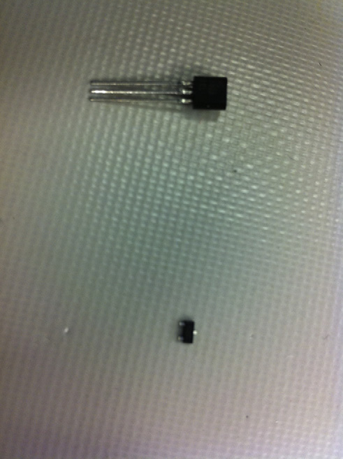
图 3.4 晶体管 SMT 与 TH 封装。#
而 PNP 则需要基极比发射极更负(更低电位)。还记得与二极管的相似性吗?它们非常相似,以至于基极到发射极的结表现得就像一个二极管,也就是说你需要克服正向压降才能让其导通。
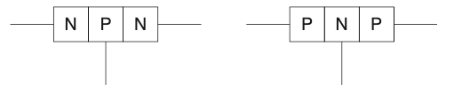
图 3.5 将二极管压合在一起形成晶体管。#
制定元件符号的那帮人让我们的生活变得轻松。他们在发射极到基极的连接处用了一个非常“二极管风格”的符号,来表明这里存在一个类似二极管的结构。还请注意,我一直在讲电流进入和流出晶体管的基极。晶体管是电流驱动器件;它们需要较大的电流流动才能工作。大多数情况下,基极所需的电流是流经集电极和发射极电流的 1/50 到 1/100,但相对于所谓的电压驱动器件,它还是显得不小。
晶体管可以用作放大器或开关。我们应该分别考虑这两种应用方式。
The next type of semiconductor is made by tacking on another type P or type N junction to the diode structure. It is called a BJT, for bipolar junction transistor, or transistor for short. One the following page is a picture of a couple common transistor packages—surface mount and through hole (Figure 3.4). They come in two flavors: NPN and PNP-—see Figure 3.5. I presume you can guess where those labels came from.
At first glance you would probably say,“Isn’t this just a couple of diodes hooked up back to back? Wouldn’t that prevent current from flowing in either direction?” Well, you would be correct. It is a couple of diodes tied together, and yes, that prevents current flow. That is, unless you apply a current to the middle part, also known as the base of the transistor. When a current is applied to the base, the junction is energized [7] and current flows through the transistor. The other connections on the transistor are called the collector and the emitter.
The NPN needs current to be pushed into the base to turn the transistor on, whereas the PNP needs current to be pulled out of the base to turn it on. [8] In other words, the NPN needs the base to be more positive than the emitter,
FIGURE 3.4 Transistor SMT and TH.#
whereas the PNP needs the base to be more negative than the emitter. Remember the similarity to the diode? It is so close that the base-to-emitter junction behaves exactly like a diode, which means that you need to overcome the forward-voltage drop to get it to conduct.
FIGURE 3.5 Smash diodes together to make a transistor.#
Whoever is in charge of making up component symbols has made it easy for us. There is a very“diode-like” symbol on the emitter-to-base junction that indicates the presence of this diode. Also, please note that I keep talking about current into and out of the base of the transistors. Transistors are current-driven devices; they require significant current flow to operate. Most times the current flow needed in the base is 50 to 100 times less than the amount flowing through the emitter and collector, but it is significant compared to what are called voltage-driven devices.
Transistors can be used as amplifiers and switches. We should consider both types of applications.
晶体管作为开关#
Transistors as Switches
在当今的数字世界中,晶体管常被用作开关,例如用来放大微控制器的输出能力。由于这是如此常见的应用,我们将讨论一些在这种方式下使用晶体管的设计指南。
In today’s digital world, transistors are often used as switches amplifying the output capability of a microcontroller for example. Since this is such a common application, we will discuss some design guidelines for using transistors in this manner.
饱和#
Saturation
当你将晶体管用作开关时,请务必考虑是否将器件驱动到饱和状态。所谓饱和,是指你向基极注入了足够的电流,使晶体管能够从集电极导出最大电流。我见过很多工程师因为晶体管无法正常工作而抓耳挠腮,最后发现原因只是基极电流不够。
When you use a transistor as a switch, always consider if you are driving the device into saturation. Saturation occurs when you are putting enough current into the base to get the transistor to move the maximum amount through the collector. Many times I have seen an engineer scratching his head over a transis- tor that wasn’t working right, only to find that there was not enough current going into the base.
选择合适的晶体管#
Use the Right Transistor for the Job
用 NPN 来开关地线,用 PNP 来开关 Vcc 电源线。乍一看你可能觉得奇怪,毕竟它们都是“开关”,对吧?没错,它们确实像开关,但由于基极的二极管压降,会产生重要差异,尤其是在你使用的是 0 到 5V 的电压范围时。请参考 Figure 3.6 中的两个设计。
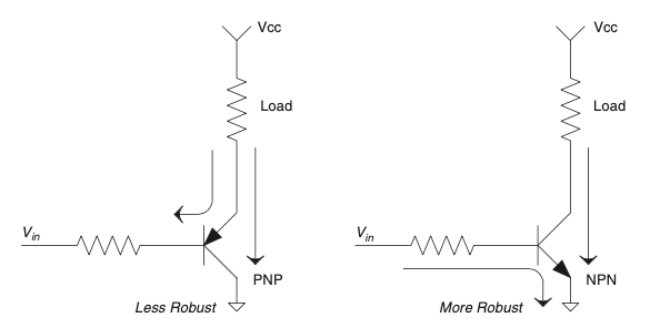
图 3.6 不同晶体管在同一电路中的比较。#
让我们对不太可靠的那个电路做一点 ISA 分析 [9]。当你降低输入电压时,电流会流向基极,但基极到发射极是个二极管,对吧?这意味着无论基极电压是多少,发射极电压总是比它高出 0.7V。即使你把输入电压降到恰好 0V,因为电流必须流动,基极电压也会稍高一些。发射极电压则会比它再高 0.7V。请注意,在这一点上的任何电压变化都会反映到输出端。现在对比更可靠的那个设计。当你将输入信号拉低时,电流也会像前一个设计那样流向基极,但你能看出区别了吗?在第二个设计中,输入电压可以有较大变化,只要晶体管处于饱和状态,输出端从集电极到发射极的电压降将保持不变。
PNP 晶体管在相反配置中表现最好(见 Figure 3.7)。在开关应用中,它在控制负载的 Vcc 电源线上更为可靠。在这两种情况下,要关闭晶体管并不难;只需将基极电压调节到距发射极 0.7V 以内,电流便会停止流动。
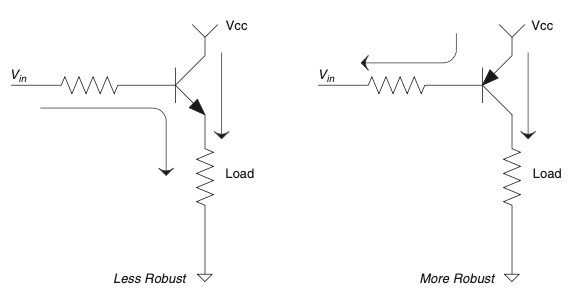
图 3.7 不同晶体管在同一电路中的比较。#
Use an NPN to switch a ground leg and a PNP to switch a Vcc leg. This might seem odd to you at first. After all, they are both like a switch, right? Well, they are like a switch, but the diode drop in the base causes an important difference, especially when you only have 0 to 5 V to deal with. Consider the two designs shown in Figure 3.6.
FIGURE 3.6 Comparison of different transistors in the same circuit.#
Let’s do a little ISA [9] on the less robust circuit. As you decrease the voltage at the input, current will flow through the base, but the emitter base junction is a diode, right? That means that whatever voltage the base is at, the emitter is always 0.7 V higher. Even if you get the input to 0 V exactly, since current has to flow, the voltage at the base will be a little higher. The voltage at the emitter will be 0.7 V above that. Notice now that any voltage change at this point will be reflected at the output. Now contrast that with the more robust design. When you pull the signal at the input low, current will flow through the base just like the other design, but do you see the difference? In the second design, the input voltage can vary quite a bit, and as long as the transistor is in satura- tion, the voltage drop at the output from collector to emitter will remain the same.
The PNP transistor works best in the opposite configuration (see Figure 3.7). For a switching application it is more robust when it controls the Vcc leg of the load. In both cases turning the transistor off is not too difficult; just get the base within 0.7 V of the emitter and the current will stop flowing.
FIGURE 3.7 Comparison of different transistors in the same circuit.#
晶体管作为线性放大器#
Transistors as Linear Amplifiers
晶体管也可以用作线性放大器。这是因为流过集电极的电流与流过基极的电流成正比 [10]。这被称为晶体管的增益 β 或 HFE。例如,如果你向基极输入 5 μA 电流,而晶体管的 β 为 100,那么你将得到 0.5 mA 的集电极电流。使这正常工作取决于保持晶体管在几个重要限制范围内操作。
一个限制来自基极到发射极连接处的二极管。该二极管需要保持正向偏置,晶体管才能线性放大。同样重要的是要避免晶体管进入饱和状态。饱和会使晶体管偏离线性区域,产生诸如削波等奇怪的结果。所有这些意味着,搭建线性晶体管放大器有一定难度。你需要注意偏置和 HFE,但遗憾的是不同器件之间 HFE 差异很大。现在我很少单独使用晶体管作为线性放大器,原因有二:第一是之前提到的器件间差异问题(这在制造数百万电路时是个大问题),第二是运算放大器(我们后面会讲)既便宜 [11] 又易用。如果你需要晶体管的功率能力,最好将它和运放配合使用,这样生活更轻松!
Transistors can also be used as linear amplifiers. This is because the amount of current flowing through the collector is proportional [10] to the current through the base. This is called the beta or HFE of the transistor. For example, if you put 5 μA into the base of a transistor with a beta of 100, you would get 0.5 mA of collector current. Making this work correctly depends on keeping the transistor operating inside a couple of important limits.
One limit is created by the diode in the base-to-emitter connection. This diode needs to remain forward-biased for the transistor to amplify linearly. It is also important to keep the transistor out of saturation. This can push the transistor out of its linear region, creating funny results such as clipping. What all this means is that setting up linear transistor amplifiers can be a bit of a trick. You need to pay attention to biasing and the HFE, which unfortunately varies considerably from part to part. These days I rarely use transistors alone as linear amplifiers for two reasons: The first is the amount of variation from part to part mentioned before (a real issue when you make millions of circuits), and the second is the fact that operational amplifiers (which we will discuss later) are so inexpensive [11] and easy to use. If you need the power capability of a transistor, you should try teaming it up with an op-amp to make life easier!
场效应晶体管#
FETs
FET,或称为 场效应晶体管,是比晶体管和二极管更新的器件(见图 Figure 3.8)。为什么要发明新东西?很简单:FET 具有一些使其非常受欢迎的特性。它们的主要优点是输出基本上是一个电阻,这个电阻随输入电压变化。FET 的输出端称为漏极和源极,输入端称为 栅极。
图 3.8 场效应管(FET)。#
几乎不需要栅极电流来控制 FET;这使得它成为放大微弱信号的理想元件,因为 FET 不会显著加载信号。事实上,一些优秀的运放就是因为这个原因在输入端使用 FET。FET 的一个缺点是比晶体管更容易损坏。它们对静电和过电压条件敏感,所以使用时务必注意其最大额定值。
FET 的一个非常酷的特性是漏极到源极的连接。它表现得像一个电阻,由栅极电压控制。实际上它是一个电子控制的可变电阻。因此,在电路中常见 FET 用于实现可变增益控制。漏极到源极连接像电阻一样对两个方向导通,电流可以双向流动。不过,FET 漏源两端通常会有一个内建的反向偏置二极管(这是 FET 结构本质决定的)。
在开关模式下,你应该关注一个术语 RDSon。这是器件全开时漏极到源极的电阻。该值越小,器件损耗的功率越少,产生的热量也越少。器件两端电压等于电流乘以 RDSon,功率耗散则是该电压乘以通过器件的电流。欧姆等于电压除以电流(如果欧姆定律仍然成立的话——到了本书这个阶段,你应该已经胸有成竹了)。欧姆的倒数 1/R 等于电流除以电压,这被称为 mho(莫)单位 [12]。对于 FET 来说,mho 就像晶体管的 β 或 HFE 一样,是其增益单位,也称为跨导。给 FET 的栅极输入 X 伏特,乘以跨导,就能得到漏极到源极的电流 Y。
与晶体管一样,输入到输出的增益在不同器件间差异较大。在使用晶体管线性放大模式时,你需要对器件进行特性测试,或采用某种反馈控制方法来补偿变化,以达到预期效果。
据我所知,有些工程师非常喜欢 FET,有些则偏爱老牌 BJT。我建议两者都放入你的工具箱,根据手头任务选用合适的工具。
FETs, or field effect transistors, were developed more recently than transistors and diodes (see Figure 3.8 ). Why come up with something new? Simple: FETs have some properties that make them very desirable components. The primary rea- son they are so slick is that the output of a FET is basically a resistance that var- ies depending on the voltage at the input. The outputs on an FET are called the drain and source, whereas the input is known as the gate.
FIGURE 3.8 The FET.#
Virtually no current is needed at the gate to control an FET; this makes it an ideal component for amplifying a signal that is weak, since the FET will not load the signal significantly. In fact, some of the better op-amps use FETs at their inputs for just this reason. One downside to an FET is that the parts tend to be easier to break than their transistor cousins. They are sensitive to static and over-voltage conditions, so be sure to pay attention to the maximum rat- ings when you use these parts.
One very cool thing about an FET is the drain-to-source connection. It acts just like a resistor that you control by the voltage at the gate. This in effect makes it an electronically controlled variable resistor. For this reason, it is common to find FETs in circuits creating variable gain control. The drain-to-source connec- tion acts like a resistor in either direction. That is, current can flow either way. However, you should expect an FET to have a built-in, reverse-biased diode across the drain-to-source pins. (It is the nature of the construction of the FET that creates this diode.)
When used in switch mode, a term you should pay attention to is RDSon. This is the resistance drain to source when the device is turned all the way on. The lower this number, the less power you will lose across the device as heat. The voltage across the device will be the current times RDSon, and the power dissi- pated in heat will be this voltage times the current through the device. An ohm equals volts divided by current if Ohm’s Law still holds true (by this point in the book, a resounding Yes! should be on the tip of your tongue). The inverse of an ohm or 1/R equals current divided by voltage. This is known as a mho. [12] Mhos are to FETs as beta or HFE is to a transistor. This is the unit of gain, also known as transconductance, that defines the output of the FET. Put X volts into the gate of the FET, multiply that by the transconductance, and you will get Y current drain to source.
Just as with transistors, this gain from input to output varies significantly from part to part. When using the transistors in linear mode, you need to either char- acterize the component you are using or develop some type of feedback control method that compensates for the variation to achieve the desired result.
In my experience, some engineers really like FETs and some like the good old BJT. I say keep both tools in your chest and use the right one for the job at hand.
印刷电路板 (PCB)#
PCB
印刷电路板不是像其他元件那样的具体元件,而是承载所有其他元件的部分。 Figure 3.9 是一个 PCB 的例子,是我自己小开发公司做的。你可能会注意到它是 SMT 和 TH 技术的结合。通常是绿色的 [13],这些部分通过所谓的线路(其实就是铜线)和过孔(连接不同层线路的孔)把元件连接起来,并通过焊接把元件固定到 PCB 上。需要记住的关键点是,这些线路具有三种基本特性:电阻、电感和电容。我们将在第4章更深入讨论元件不完美时的影响,但我现在给你一个提示:你首先需要问,这些线路特性是否足够显著,以至于对线路上的信号产生影响?在高频时,这些效应可能非常重要;而在低频时则影响较小。有许多专门讲 PCB 布局方法的书籍,这里我们不展开讲。我只希望你意识到 PCB 本身和上面的元件一样,都是电路的一部分。千万别忘了这一点。
图 3.9 一个 PCB。#
The printed circuit board is not a specific component like the rest, but the part that carries all the other parts. Figure 3.9 is an example of a PCB, one from my very own little development company. You might notice that it is a combination of SMT and TH technology. Often green in color [13] these parts connect the other parts together using things called traces (the lines that are really copper wires), and vias (holes that connect layers of traces together) solder to connect the parts to the PCB. One key item to remember is that these traces have all of the three basic components, that is, resistance, inductance, and capacitance. We will cover this in more depth in Chapter 4 when parts aren’t perfect, but one hint that I will give now is you need to ask first, is it enough to matter given the signals that are on these traces? At higher frequencies these effects can be very significant, at lower values not so much. There are plenty of tomes dedicated to PCB layout methodol- ogies so we won’t get into that depth here. I only hope to help you realize that the PCB itself is as much a part of your circuit as all the components on it. Don’t forget that.
FIGURE 3.9 A PCB.#
附加零件随机列表#
Random List of Additional Parts
这里列出了一些你可能听说过也可能没听过的半导体零件:
备注
- 达林顿晶体管(Darlington transistor)。
这种晶体管由两个晶体管串联组成,以提高增益,从其符号即可看出。注意,达林顿晶体管中基极-发射极的二极管压降基本上是两倍。
- 硅控整流器(SCR)。
当你创建一个 PNPN 结时,就得到了硅控整流器。它基本上是二极管和晶体管的结合,能轻松切换大电流。但有一点警告——你可以打开它但不能关闭它。通过 SCR 的电流必须降到保持电流(非常小)以下,它才会自行关闭。SCR 属于晶闸管家族。TRIAC 是 SCR 的“表亲”,也属于晶闸管家族。可以把它看成两个 SCR 背靠背,使其成为一个有效的交流开关。它经常出现在固态继电器等设备中。
- 绝缘栅双极晶体管(IGBT)。
绝缘栅双极晶体管最好理解为晶体管和场效应管的结合体。用场效应管推动电流负载通过一个大晶体管。
半导体的变化其实并不多;它们基本上是 P 型和 N 型材料的几种基础组合。让我惊讶的是,仅靠几个部分就能实现如此复杂的功能,半导体真正革新了我们今天的世界。不过,细节决定成败。我再三强调,一定要认真阅读你使用的器件的数据手册。你对器件的各种特性了解得越多,设计就会越好。
经验法则
二极管是电子的“单向阀”。
二极管有一个必须克服的正向压降,才能导通。
晶体管是电流驱动的。
晶体管基极有一个二极管,需要偏置才能正常工作。
用晶体管做开关时,要检查饱和电流。
场效应管是电压驱动的。
场效应管相对脆弱;设计时要留出足够裕度,确保电路工作在器件最大额定值以内。
场效应管对静电敏感。
认真研读你使用器件的数据手册。
PCB 线路具有三种基本特性:电阻、电感和电容。
Here are a few parts in the semiconductor world that you may or may not have heard of:
备注
- Darlington transistor.
This type of transistor consists of two transistors hooked together to increase the gain, as can be seen by the symbol used to represent it. Note that the base emitter diode drop is basically doubled in a Darlington transistor.
- SCR.
This is what you get when you create a PNPN junction, called a silicon- controlled rectifier. Basically the combination of a diode and a transistor, it can switch large currents easily. But one caveat—you can turn it on but not off. The current through the SCR must get below the holding current (very small) before it turns itself off. The SCR is part of the thyristor family. TRIAC. This is a cousin to the SCR and also is in the thyristor family. Think of it as two SCRs back to back, making it an effective AC switch. It is often found in solid-state relays and the like.
- IGBT.
The isolated gate bipolar transistor is best thought of as a combination between a transistor and an FET. An FET is used to push a load of current through a big transistor.
There aren’t really a lot of different variations in semiconductors; they all boil down to some basic configurations of the P and N materials. It is amazing to me that such a level of complexity is achieved from just a few parts, but semi- conductors have truly revolutionized the world as we know it today. The devil is in the details, however. I can’t stress too much the need to look at the data- sheet of the part you are using. The more you know about its idiosyncrasies, the better your designs will be.
Thumb Rules
Diodes are a“one-way” valve for electrons.
Diodes have a forward-voltage drop you must overcome before they will conduct.
Transistors are current driven.
Transistors have a diode in the base that needs to be biased to work right.
When using transistors as switches, check saturation current.
FETs are voltage driven.
FETs tend to be less robust; take care to design plenty of headroom between your circuit and the maximum ratings of the part.
FETs are static sensitive.
Meticulously study the datasheet of the part you are using.
PCB traces have the three basic components: resistance, inductance, and capacitance.
功率与热管理#
POWER AND HEAT MANAGEMENT
所有电气设备(超导体除外)都有一个共同点:运行时会产生热量。这是因为每个元件中(我们后面会学习)都有一定的等效电阻。
电阻乘以电流等于电压降,电压降乘以电流等于功率。既然欧姆定律不可避免,这些功率必须转化为热量。热量是电子元件磨损的主要原因,所以管理热量是很重要的。让我们从内部开始说起。
One thing in common with all electrical devices (this side of superconductors) is the fact that as they operate, heat is generated. This is because in every component (as we will learn later) there is some amount of equivalent resistance.
Resistance times current flow equals a voltage drop, and a voltage drop times current equals power. Since Ohm’s Law is unavoidable, this power must turn into heat. Heat is the premier cause of wear and tear in electronic components, so managing heat is a good thing to know something about. Let’s start from the inside out.
结温#
Junction Temp
半导体内部,所有神奇发生的地方,叫做结点(junction)。这是元件工作时产生热量的源头。结点有一个最大允许温度,超过这个温度就会出问题。没错,要知道它能承受多少热,必须查看器件的数据手册。
Inside a semiconductor, the place where all the magic happens, is called the junction. This is the point where all the heat comes from as the part operates. The junction will have a maximum temperature that it can reach before some- thing goes wrong. You guessed it; you find out just how much it can handle by reading the datasheet for the part.
封装温度#
Case Temp
结点总是在某种封装内部。设计测试时你无法测量结点温度,只能测量封装温度。结点温度总是高于封装温度。这个温差通常会在数据手册里给出。如果手册上说封装到结点的热阻导致温差为 15°C,那结点温度就比你测量的封装温度高 15°C。这里就体现了好工程师的技巧。如果老板让你把器件工作温度压到极限,你可以告诉她根据数据手册你必须保持结点温度低 30°C。她大概不会知道去哪里找这个信息,可能会相信你,而你也能得到更稳健的设计。
The junction is always inside some type of case. Since you can’t measure junction temperature when you need to test a design, you have to measure case tempera- ture. There will always be a temperature drop from the junction to the case. The amount will typically be indicated in the part’s spec sheet. If it says the case-to-junction thermal drop is 15°C, expect the junction temp to be 15° warmer than what you measure. Here is where a good engineer will fudge the numbers in his favor. If the boss asks you to run this part as close to the edge as possible, tell her you need to be 30° under the junction temp per the spec sheet. Most likely she won’t know where to look for this information, so will probably believe you and you will have a more robust design.
散热器#
Heat Sinking
封装温度的高低取决于其散热器的好坏。封装本身可以将一定热量辐射到周围空气。如果这不够用,可以增加散热器。你应该明白,散热器(名字看似会“吸走”热量)其实不是一个能让热量“倒进去”的洞。更准确地说,散热器是更有效地将热量传递到周围环境(通常是空气)的一种方式。
散热器捕捉热量并把它散发到周围空气。散热器有一个单位 °C/W,表示每瓦热功率会使器件温度升高多少摄氏度。例如,20 瓦热功率加到一个 3°C/W 的散热器上,器件温度会比环境温度高 60°C。
散热器可以被看作是热的导体。就像有些金属比其他金属导电更好一样,有些金属导热更好,通常二者相伴。铝比钢导电更好,也比钢导热好。铜是最好的导电体之一,同时也是最好的导热体之一。这样看,散热器就是把热量从器件导走。就像电流总是从高电势流向低电势,热量也总是从高温流向低温。热传递有几种方式,我们接下来会讲。
How hot the case gets depends on the heat sink attached to it. The case itself will be able to radiate a certain amount into the air around it. If this isn’t sufficient, a heat sink can be added. One point you should recognize is that a heat sink (contrary to what you might think, given the name) is not a hole into which you can dump the heat from the part. A heat sink is more accurately described as a way to more efficiently transfer heat into the surrounding environment (this happens to be the air in most cases).
Heat sinks capture that thermal rise and dissipate it into the surrounding air. Heat sinks are rated by a°C/W number. This number represents how much the temperature of the device on the sink will rise for every watt of heat gen- erated. For example, if you put 20 watts of heat on a 3°C/W heat sink, the power device hooked up to that heat sink will rise 60°C above the ambient temperature.
Heat sinks can be thought of as heat conductors. Just as some metals are better electric conductors than others, some metals are better heat conductors. Usually one goes with the other. Aluminum is a better electrical conductor than steel, and it is also a better heat conductor. Copper, one of the best electrical conductors around, is also one of the best heat conductors. Thought of in these terms, the heat sink conducts heat away from the part. Like the fact that current always flows in one direction, heat always flows from hot to cold. There are a couple of ways for this to happen, as we will see now.
辐射#
Radiation
当散热器变热后,它会发出红外辐射;随着能量的辐射,散热器会降温。你有没有想过为什么很多散热器是黑色的?这是因为黑色 [14] 是高效的辐射体,这种颜色能吸收更多红外线(如果你曾在阳光下穿黑色衣服应该有所体会)。只要散热器所在环境较冷且没有阳光直射,它就能把热量辐射走。尽管辐射是散热的一种方式,但在大多数现代电子设备中还有更好的散热方式。
Once the heat sink is warm, it will emit infrared radiation; as this energy is radiated away, the heat sink will cool. Have you ever wondered why so many heat sinks are black? This is because the color black [14] is an efficient radiator, as this color tends to absorb more infrared radiation (as you probably have noticed if you have ever worn a black shirt on a sunny day). It will radiate this heat away as well, as long as the part is in a cooler environment and the sun isn’t shining on it! Although radiation is a way of getting heat moving away from your part, in most electronic devices today there are much better ways to get rid of heat.
对流#
Convection
散热的最好方式是让空气流过散热器,这叫做对流。有两种方式实现对流:一种是将散热器放置在使其附近的暖空气上升的位置。当暖空气上升时,较冷的空气会取代它的位置被加热,整个过程不断循环。(参见 Figure 3.10。)大多数散热器都会有自由空气散热的规格,描述其性能。
图 3.10 散热器上的对流。#
顺带一提:自由空气对流依赖重力(没有重力,热空气不会上升被冷空气替代),所以如果你正在做航天飞机实验,别指望自由空气对流来降温!
通过增加空气流速可以极大提升散热效果。通常通过风扇实现。常见的情况是,仅仅加个风扇,散热器就能承受十倍的功率。这也是如今许多设备都会发出风扇嗡嗡声的原因。
散热器与空气接触的面积越大,散热越好。因此,这些器件通常有许多散热鳍片。鳍片越多,表面积越大,散热效率越高。
嗯,这里有个想法:如果能回收这些热量并转成电能该多好?我知道有热电器件加热时会发电,这想法似乎很简单。我想我以后会设计这样的装置,如果你们中有人先实现并赚了大钱,求1%分成!
The best way to get rid of heat is by moving some air across your heat sink. This is called convection. There are two ways to achieve convection: one is by placing the sink so that air that is warmed by proximity to the heat sink rises. As this happens, cooler air takes its place to be warmed up and the whole process repeats. (See Figure 3.10.) Most heat sinks have some type of spec as to free- air operation that describes their function in this case.
FIGURE 3.10 Convection on a heat sink.#
One quick side note: Free-air convection relies on the presence of gravity (hot air won’t rise to be replaced by the cooler air without gravity), so if you happen to be working on a space shuttle experiment, don’t count on free-air convection for cooling!
A huge difference in cooling a heat sink can be achieved by moving more air across it. This is commonly accomplished by some type of fan. It is not unusual to see a heat sink handle 10 times as much power just by placing a fan next to it. This is the reason that so many devices these days have acquired that prover- bial hum of a fan that is so prevalent.
The more heat sink area you have in contact with the air, the better it can trans- fer heat. For this reason, you will see a lot of fins on these parts. More fins mean more surface area, which means more efficient heat transfer.
Hmmm, here’s a thought: Wouldn’t it really be nice to recapture this heat and turn it back into power? I know there are thermoelectric devices that generate electricity when you heat them up, so this seems like a no-brainer. I guess I will get to that design later, but if any of you reading this get to the punch before me and make millions with this idea, all I ask is 1%!
传导#
Conduction
传导是另一种传递热量的方式。这是热量从器件传到散热器的方式,也是热量沿散热器传播的方式。传导非常有效(这就是热量从器件传到散热器的途径),但热量只能从温度高的地方流向温度较低的地方。通常用液体来传导热量,比如核反应堆或汽车发动机。但最终热量必须排到某处,所以你看到汽车前面有散热器,将防冻液带走的热量散发到空气中。我的船的发动机用整个湖泊作为散热器,不需要散热器,因为显然我的小船没有足够功率将数百万加仑水温度提高哪怕一小部分。 [15]
Another way of moving heat is by conduction. This is how the heat gets from the part into the heat sink, and it is how the heat travels across the sink as well. Conduction moves heat very, very well (that is how it gets from the part into the heat sink), but whatever it is conducting to must be cooler than where the heat is coming from in order for the heat to flow. Often a liquid is used to conduct heat away from stuff that gets hot, such as a nuclear reactor or your car engine. At the end of the day, though, that heat has to go some- where. That’s why you see a radiator in the front of your car dumping all that heat collected by the antifreeze into the atmosphere. The engine in my boat uses the entire lake as a heat sink, with no radiator needed, since it should be fairly obvious that my piddling little boat isn’t going to have enough power to raise the average temperature of millions of gallons of water by even a fraction of a degree. [15]
可以用PCB来散热吗?#
Can You Dump It into a PCB?
这是我经常听到的问题:能用 PCB 作为散热器吗?答案是肯定的。PCB 其实就是铜箔,我们知道铜是良好的导热体,所以它可以用来散热。好,现在来了……但是……你怎么知道 PCB 散热到空气的效率呢?这个大多数情况下得靠测试才能弄清。计算时变量太多,最快的方法是做出 PCB,装上器件,实测。以下是用 PCB 作为散热器时需要注意的事项:
许多连接顶层和底层的小过孔能增加散热面积。
PCB 在此区域会变热,会发生膨胀和收缩,长时间可能造成机械损伤,甚至焊点和线路断裂。
我建议 PCB 散热区温度控制在 60°C 以下。我学到的一个经验法则是,金属表面烫手说明温度超过 60°C。 [16]
This is a question that I have often heard: Can you use the PCB as a heat sink? The answer is yes. In fact, the PCB is simply copper plating, and we know that copper is a good heat conductor, so it follows that it can be used as a heat sink. Okay, here it comes… but… how do you know how well the PCB radiates the heat into the atmosphere? That is something you will most likely have to test to figure out. There are just so many variables in calculating this that it is faster to lay out the PCB, stick the part on, and try it. Here are some items to note when you’re using a PCB as a heat sink:
A lot of little vias connecting the top layer to the bottom one will help increase the amount of surface area you have to dissipate the heat.
The PCB in this area is going to get warm. That means expansion and contraction of the PCB. You might find that this could cause mechanical damage over time or even crack solder joints and PCB connections.
I would recommend keeping the PCB heat sinks under 60°C. A cool rule of thumb I have learned is that if a metal surface is hot enough to burn you at the touch, it is more than 60°C. [16]
散热扩散#
Heat Spreading
两个材料紧密接触时,控制热传导的一个重要因素是它们接触面的面积。另一个影响单一材料传导的因素是材料的厚度。
这就产生了散热扩散技术。用一个大且厚、热导率高的材料紧贴“热源”,作为高速导热通道连接到更大的散热器,后者带有大量鳍片用来辐射热量。 [17] 其目的是通过更快散热保持器件结温较低。
问这方法有效吗?实际上可以,但涉及许多变量(比如散热扩散块与散热器其余部分之间的热导率)。像用 PCB 做散热器一样,你应送实验室检测,看看效果到底如何。记住,任何两个零件接触处都会有温度梯度;接触面越少,散热效果越好。
经验法则
认真研读你使用器件的数据手册(再次强调)。
热量是电子元件的最大杀手。
大多数散热器通过对流向周围空气散热。
如果摸到元件会烫手,说明温度超过 60°C。
可以用 PCB 作为散热器,但要小心测试。
One of the major factors that control heat conduction when you have two materials next to each other is the surface area of the two materials that are touching. One other thing that affects conduction of a single material is the thickness of the material.
This gives rise to a technique known as heat spreading. A big, thick, very ther- mally conductive material is bolted up to the“hot part” to serve as a high-speed conduit to a bigger heat sink, where all the fins for radiating the heat are located. [17] The idea is to keep the junction temperature of the device lower by getting the heat away faster.
Does it work, you ask? Truth is, it can work, but there are many variables involved (such as the thermal conductivity between the heat spreader block and the rest of the heat sink, for example). As in the case of using the PCB as a heat sink, you should take it to the test lab to see if it is really working well or even helping. Remember, though, there will be a temperature gradient everywhere that there is a junction between two parts; the fewer junctions, the better your heat sink will work.
Thumb Rules
Meticulously study the datasheet of the part you are using (repeated for emphasis).
Heat is the biggest killer of electronic components.
Most heat sinks dump heat into the air around them, most commonly by convection.
If a part burns you when you touch it, it is more than 60°C.
You can use a PCB as a heat sink, but take care to test it.
神奇又神秘的运算放大器#
THE MAGICAL MYSTERIOUS OP-AMP
运算放大器:被误解的神奇工具!#
Op-Amps: The Misunderstood Magical Tool!
在我看来,运算放大器可能是工程师手中最被误解但又最有潜力的集成电路。如果你能理解这个器件,就能有效利用它,在设计成功产品时占据巨大优势。
In my opinion, op-amps are probably the most misunderstood yet potentially useful IC at the engineer’s disposal. It makes sense that if you can understand this device, you can put it to use, giving you a great advantage in designing suc- cessful products.
什么是运算放大器?#
What Is an Op-Amp, Really?
你了解运算放大器的工作原理吗?你会相信运算放大器是为了简化电路设计而发明的吗?上次你在实验室苦恼于面包板电路出错时,可能没这么想过。
在当今数字化的世界里,运算放大器的内容往往被匆匆带过,只给学生一些常用公式,却很少解释其目的和背后的理论。于是新工程师第一次设计运算放大器电路时,电路不按预期工作,结果一头雾水。本文旨在深入剖析运算放大器的内部结构,帮助读者直观理解运算放大器。
图 3.11 你的基础运算放大器。#
最后一点:一定要先读这一节!我认为“运放迷惑症”(我称之为“op-fusion”)的原因之一是理论讲解顺序错乱。学习理论有严格顺序,请务必理解每节内容再继续。首先看运算放大器的符号(见 Figure 3.11)。有两个输入,一个正(+),一个负(-),还有一个输出。
输入阻抗很高。我再说一遍,输入阻抗很高。再强调一次,输入阻抗很高!这意味着它们对所连接电路几乎没有影响。请记下来,这非常重要。后面会详细讲解。这个重要事实常被忽略,也是造成之前提到混淆的原因。
输出阻抗很低。大多数分析中,最好将其视为电压源。现在用两个独立符号表示运算放大器,如 Figure 3.12 所示。
这里你看到一个求和块和一个放大块。你可能在控制理论课上见过类似符号。实际上,它们不仅相似——完全相同。控制理论同样适用于运算放大器。(后面还会详细讲。)
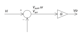
图 3.12 运算放大器内部结构。#
先讲求和块。你会注意到求和块上有正输入和负输入,就像运算放大器一样。负输入相当于该点电压乘以 -1。因此,如果正输入是 1 V,负输入是 2 V,则该块输出为 -1。这个输出是两个输入的和,其中一个输入乘以 -1。也可看作两个输入的差,公式如下:
接下来是放大块。块内变量 G 表示运算放大器对输入电压和的放大倍数,也称开环增益。这里取值 50,000。我听你说:“怎么可能?我用运算放大器做的放大电路没这么大增益!”请先相信我。后面会讲放大应用。你可以查厂商数据手册,开环增益通常有这么大甚至更高。
做个分析。如果正输入为 2 V,负输入为 3 V,输出会怎样?建议你在面包板上实际测试,看看运放能否输入不同电压正常工作。不过数学和常识会告诉我们结果,例如:
除非你用连接 50,000 V 电源的 50,000 V 运放,否则不会看到 -50,000 V 输出。你会看到什么?想想再看下面。输出会达到最小电源轨。换句话说,会尽可能向负方向摆。这样想很合理:输出想要到达 -50,000 V,符合数学计算,但做不到,只能尽量接近。运放的电源轨就像铁轨,火车会尽量不出轨。运放若被逼出轨,芯片就会损坏,神奇的烟雾会冒出。电源轨是运放能输出的最大和最小电压。你也能理解,这取决于电源和运放具体性能。好了,把输入反过来,结果变为:
这时输出会达到最大电源轨。怎么知道运放的电源轨范围?如前所述,取决于你用的电源和运放型号,要查厂商手册。假设用 LM324,单电源 +5 V,输出负向接近 0 V,正向接近 4 V。
这里想指出一点:运放输入端电压不一定相等。我经常见到工程师误以为两输入端电压应相同。分析时他们假设输入端有电流让电压相同(记住,高阻抗输入,几乎无电流)。实际测试时,测得输入电压不同,令他们困惑。
在下一节讨论的特殊情况下,可以假设两输入相等。但这不是通用情况!这是常见误解,千万别陷入此陷阱,否则根本无法理解运算放大器。
前面例子展示了运算放大器一个很棒的应用:比较器电路。这是将模拟信号转换为数字信号的好电路。用它可判断一个输入信号是否高于另一个。事实上,许多微控制器的模数转换过程中用到了比较器电路。比较器电路无处不在。你想街灯怎么知道天黑该开灯?它用比较器连接光传感器。红绿灯怎么知道路面有车触发绿灯?肯定有比较器电路。
经验法则
输入阻抗高,对连接的电路几乎无影响。
两输入端电压可以不同,不必相等。
运算放大器开环增益很高。
由于高开环增益和输出限制,如果一输入高于另一输入,输出会飙到最大或最小电压轨。(这就是所谓比较器电路。)
Do you understand how an op-amp works? Would you believe that op-amps were designed to make it easier to create a circuit? You probably didn’t think that the last time you were puzzling over a misbehaving breadboard in the lab.
In today’s digital world it seems to be common practice to breeze over the topic of op-amps, giving the student a dusting of commonly used formulas without really explaining the purpose or theory behind them. Then the first time a new engineer designs an op-amp circuit, the result is utter confusion when the cir- cuit doesn’t work as expected. This discussion is intended to give some insight into the guts of an operational amplifier and to give the reader an intuitive understanding of op-amps.
FIGURE 3.11 Your basic op-amp.#
One last point: Make sure that you read this section first! It is my opinion that one of the causes of“op-fusion” (op-amp confusion), as I like to call it, is that the theory is taught out of order. There is a very specific order to learning the theory, so please understand each section before moving on. First, let’s take a look at the symbol of an op-amp (see Figure 3.11). There are two inputs, one positive and one negative, identified by the + and – signs. There is one output.
The inputs are high impedance. I repeat. The inputs are high impedance. Let me say that one more time. The inputs are high impedance! This means that they have (virtually) no effect on the circuit to which they are attached. Write this down because it is very important. We will talk about this in more detail later. This important fact is commonly forgotten and contributes to the confusion I mentioned earlier.
The output is low impedance. For most analyses it is best to consider it a voltage source. Now let’s represent the op-amp, as in Figure 3.12, with two separate symbols.
You see here a summing block and an amplification block. You may remem- ber similar symbols from your control theory class. Actually, they are not just similar—they are exactly the same. Control theory works for op-amps. (There will be more on this topic coming up later.)
FIGURE 3.12 What is really inside an op-amp?#
First, let’s discuss the summing block. You will notice that there is a positive input and a negative input on the summing block, just as on the op-amp. Recognize that the negative input is as though the voltage at that point is multiplied by–1. Thus, if you have 1 V at the positive input and 2 V at the negative input, the output of this block is–1. The output of this block is the sum of the two inputs where one of the inputs is multiplied by–1. It can also be thought of as the difference of the two inputs and represented by this equation:
Now we come to the amplification block. The variable G inside this block represents the amount of amplification that the op-amp applies to the sum of the input voltages. This is also known as the open-loop gain of the op-amp. In this case, we will use a value of 50,000. I hear you say,“How can that be? The amplification circuit I just built with an op-amp doesn’t go that high!” Just trust me for a moment. We will get to the amplification applications shortly. Just go find the open-loop gain in the manufacturer’s datasheet. You will see this level of gain or even higher is typical of most op-amps.
Now let’s do a little analysis. What will happen at the output if you put 2 V on the positive input and 3 V on the negative input? I recommend that you actually try this on a breadboard. I want you to see that an op-amp can and will operate with different voltages at the inputs. However, a little math and some common sense will also show us what will happen. For example:
Now, unless you have a 50,000 V op-amp hooked up to a 50,000 V bipolar sup- ply, you won’t see–50,000 V at the output. What will you see? Think about it a minute before you read on. The output will go to the minimum rail. In other words, it will try to go as negative as possible. This makes a lot of sense if you think about it like this. The output wants to go to–50,000 V and obey the preceding mathematics. It can’t get there, so it will go as close as possible. The rails of an op-amp are like the rails of a train track; a train will stay within its rails if at all possible. Similarly, if an op-amp is forced outside its rails, dis- aster occurs and the proverbial magic smoke will be let out of the chip. The rail is the maximum and minimum voltage the op-amp can output. As you can intuit, this depends on the power supply and the output specifics of the op-amp. Okay, reverse the inputs. Now the following is true:
What will happen now? The output will go to the maximum rail. How do you know where the output rails of the op-amp are? As noted before, that depends on the power supply you are using and the specific op-amp. You will need to check the manufacturer’s datasheet for that information. Let’s assume that we are using an LM324, with a +5 V single-sided supply. In this case, the output would get very close to 0 V when trying to go negative and around 4 V when trying to go positive.
At this time I would like to point something out. The inputs of the op-amp are not equal to each other. Many times I have seen engineers expect these inputs to be the same value. During the analysis stage, the designer comes up with currents going into the inputs of the device to make this happen (remember, high impedance inputs, virtually zero current flow). Then when he tries it out, he is confused by the fact that he can measure different voltages at the inputs.
In a special case we will discuss in the next section, you can make the assumption that these inputs are equal. It is not the general case! This is a common misconception. You must not fall into this trap or you will not understand op-amps at all.
The previous examples indicate a very neat application of op-amps: the comparator circuit. This is a great little circuit to convert from the analog world to the digital one. Using this circuit you can determine whether one input signal is higher or lower than another. In fact, many microcontrollers use a comparator circuit in analog-to-digital conversion processes. Comparator circuits are in use all around us. How do you think the streetlight knows when it is dark enough to turn on? It uses a comparator circuit hooked up to a light sensor. How does a traffic light know when there is car present above the sensors to trigger a cycle to green? You can bet there is a comparator circuit in there.
Thumb Rules
The inputs are high impedance; they have negligible effects on the circuit to which they are hooked.
The inputs can have different voltages applied to them; they do not have to be equal.
The open-loop gain of an op-amp is very high.
Due to the high open-loop gain and the output limitations of the op-amp, if one input is higher than the other, the output will“rail” to its maximum or minimum value. (This application is often called a comparator circuit.)
负反馈#
NEGATIVE FEEDBACK
如果你还没读完上一节的经验法则,请回去先读一遍。它们对于正确理解运算放大器的功能非常重要。为什么这些点很重要?让我们回顾一点历史。
在运算放大器发明之前,工程师只能使用晶体管来做放大电路。晶体管的问题在于,它们是“电流驱动”器件,总会通过负载电路来影响设计者想放大的信号。另外,由于晶体管制造公差,电路增益会有显著变化。总之,设计放大电路是个繁琐且反复试验的过程。工程师们想要的是一种简单器件,能直接连接信号,将其放大到任意想要的倍数,而且易用,外部元件少。换句话说,操作这类放大器应该“轻而易举”。这也是“运算放大器”名字的由来之一——这种放大器被用于模拟计算机中执行乘法等运算。
首先,回到上一节提到的特殊情况。回看之前的框图,加上反馈环路,如 Figure 3.13 所示。
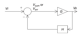
图 3.13 负反馈的原始运算放大器符号。#
这里我用 G 表示开环增益,用 H 表示反馈增益。你首先应注意输出连接到负输入,这称为负反馈。负反馈有什么用?做个实验:将手悬空一寸在桌上保持不动。你此刻正体验负反馈。通过视觉和触觉,你感知手与桌子的距离。如果手动了,你会反方向调整。这就是负反馈。你将感官接收的信号反向反馈到手臂。运放中也一样,输出信号反馈到负输入。输出信号向一个方向变化时,Vsum 会向相反方向变化。
你应该直观理解这个负反馈配置。看上图,假设 G=50000,H=1。先给正输入加 1 V,假设负输入初始为 0。此时,增益块 G 输入为 1,输出开始向正电源轨靠近。但当输出接近 1 时,负输入也接近 1。求和块输出变得越来越小。如果负输入超过 1,增益块输入将变负,迫使输出往负方向走。当然,这会导致增益块输入出现正误差,过程又开始循环。最终会停在哪里?当负输入等于正输入时停。这里 H=1,所以输出也为 1。
你会(或已经)在控制理论中学过。看与 Figure 3.13 相关的基本控制方程:
当 G 很大时会怎样?[18] 分母中的 1 可忽略,方程变为:
这里 H 是 1,[19] 所以:
即:
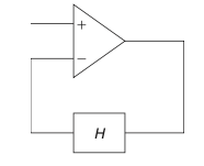
图 3.14 负反馈的原始运算放大器符号。#
这就是你可以假设运放输入相等的特殊情况。仅当存在负反馈时才适用。当反馈增益为 1 时,也展示了另一种巧妙的运放电路:电压跟随器。无论正输入电压是多少,输出都会跟随。
看 图 3.14,这是一种负反馈配置的运放。你应看到一个求和器和放大器,就像前面那幅图一样。在此配置下,你可以假设正负输入相等。
负反馈是学校里反复强调的情况,也是最常用但常引起困惑的情况。它是一个特殊情况——非常广泛使用的特殊情况。尽管如此,如果没有负反馈且输入输出在工作范围内,切勿假设运放输入相等。
为什么负反馈配置被广泛使用?记住运放发明的初衷吗?放大器很难设计,必须有更简单的方法。再看控制方程:
我已经展示当 G 很大时方程近似为:
你会看到 Vi 的放大倍数由 H 决定。例如,如果 H=1/10,则:
即:
我们如何实现?还记得分压电路吗?这里非常有用,因为我们想让 H 等于除以 10。让我们用分压电路替代 H。
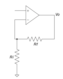
图 3.15 负反馈是电压分压器。#
注意,分压电路输入来自运放输出 Vo,分压输出接负输入 V–。那么运放负输入 V– 会影响分压电路吗?不会!因为输入阻抗高,不影响分压器。(没懂请回头读“什么是运算放大器?”章节,直到理解!)
因为分压输入接电压源,输出不受电路影响,我们可以用分压规则轻松算出 Vo 到 V– 的增益,如 Figure 3.15 所示:
因此:
用代数变形:
这就是该运放电路的增益。换个角度看,回到前式:
负反馈特殊情况下,可假设 V– = V+。这是因为负反馈环路推动输出达到此状态。设 Vi= V–,即放大器输入端。将 V+ 替换为 Vi,方程变为:
我们真正想知道的是,电路对 Vi 产生怎样的 Vo?做点数学推导:
注意,这正是 1/H。你看,这电路的增益由两个简单电阻控制。相信我,这比晶体管放大电路更易计算。可见,这种放大器的操作非常易懂。
经验法则
只有负反馈配置时,才可假设
V– = V+。高阻抗输入和低阻抗输出使得反馈环路中简单电阻网络的影响易于计算。
运放高开环增益使得该特殊情况下输出增益约等于 1/H。
运算放大器的设计初衷是简化放大,别让它变复杂!
If you didn’t just finish reading them, go back and read the last section’s thumb rules. They are very important in developing a correct understanding of what an op-amp does. Why are these points important? Let’s go over a little history.
Up until the invention of op-amps, engineers were limited to the use of transistors in amplification circuits. The problem with transistors is that, being“current-driven” devices, they always affect the signal of the circuit that the designer wants to amplify by loading the circuit. Also, due to manufacturing tolerances of transistors, the gain of the circuits would vary significantly. All in all, designing an amplifier circuit was a tedious process that required much trial and error. What engineers wanted was a simple device that they could attach to a signal that could multiply the value by any desired amount. The device should be easy to use and require very few external components. To paraphrase, operation of this amplifier should be a“piece of cake.” At least that is the way I remember it. The other way the name operational amplifier, or op-amp, came into being was to describe the fact that these amplifiers were used to create circuits in analog compu- ters, performing such operations as multiplication, among others.
To begin with, let’s take a look at the special case I mentioned in the previous discussion. First, return to the previous block diagram and add a feedback loop, as shown in Figure 3.13.
FIGURE 3.13 Original op-amp symbol with negative feedback.#
You will see that I have represented the forward or open-loop gain with the value G and the feedback gain with the value H. The first thing you should notice is that the output is tied to the negative input. This is called negative feedback. What good is negative feedback? Let’s try an experiment. Hold your hand an inch over your desk and keep it there. You are experiencing negative feedback right now. You are observing via sight and feel the distance from your hand to the desk. If your hand moves, you respond with a movement in the opposite direction. This is negative feedback. You invert the signal you receive via your senses and send it back to your arm. The same thing occurs when nega- tive feedback is applied to an op-amp. The output signal is sent back to the negative input. A signal change in one direction at the output causes a Vsum to change in the opposite direction.
You should get an intuitive grasp of this negative feedback configuration. Look at the previous diagram and assume a value of 50,000 for G and a value of 1 for H. Now start by applying a 1 to the positive input. Assume that the negative input is at 0 to begin with. That puts a value of 1 at the input of the gain block G and the output will start heading for the positive rail. But what happens as the output approaches 1? The negative input also approaches 1. The output of the summing block is getting smaller and smaller. If the negative input goes higher than 1, the input to the gain block G will go negative as well, forcing the output to go in the negative direction. Of course, that will cause a positive error to appear at the input of the gain block G, starting the whole process over again. Where will this all stop? It will stop when the negative input is equal to the positive input. In this case, since H is 1, the output will also be 1.
You have learned (or will learn) this in control theory. Look at the basic control equation in reference to Figure 3.13:
What happens when G is very large? [18] The 1 in the denominator becomes insignificant and the equation becomes:
H in this case is 1, [19] so it follows that:
or:
FIGURE 3.14 Original op-amp symbol with negative feedback.#
This is the special case in which you can assume that the inputs of the op-amp are equal. Apply it only when there is negative feedback. When feedback gain is 1, this also demonstrates another neat op-amp circuit: the voltage follower. Whatever voltage is put on the positive input will appear at the output.
Take a look at Figure 3.14. This is an op-amp in the negative feedback configuration. When you look at this, you should see a summer and an amplifier, just as in the previous drawing. In this configuration, you can make the assumption that the positive and negative inputs are equal.
Negative feedback is the case that is drilled into you in school and is the one that often causes confusion. It is a special case—a very widely used special case. Nonetheless, if you do not have negative feedback and the inputs and output are within operational limits, you must not assume that the inputs of the op-amp are equal.
Why is this negative feedback configuration used so much? Remember the rea- son that op-amps were invented? Amplifiers were tough to make. There had to be an easier way. Take a look at the control equation again:
I have already shown that for large values of G, the equation approximates:
You will see that the amplification of Vi depends on the value of H. For example, if we can make H equal 1/10, then it follows that:
or:
How do we go about doing that? Do you remember the voltage divider circuit? That would be very useful here, since we would like H to be the equivalent of dividing by 10. Let’s insert the voltage divider circuit in place of H.
FIGURE 3.15 Negative feedback is a voltage divider.#
Notice that the input to the voltage divider comes from the output of the op-amp Vo. The output of the voltage divider goes to the negative input of the op-amp V–. Now, will the op-amp input V– affect the voltage divider circuit? No! It has high impedance. It will not affect the divider. (If you didn’t get that, go back and read the“What Is an Op-Amp, Really?” section’til you do!)
Since the input to the divider is hooked to a voltage source, and the output is not affected by the circuit, we can calculate the gain from Vo to V– very easily with the voltage divider rule shown in Figure 3.15.
Thus it follows that:
or, with a little algebra:
There you have it—the gain of this op-amp circuit. Let’s look at it another way. Go back to the previous equation:
We learned that in this special case of negative feedback, we can assume that V– = V+. This is because the negative feedback loop is pushing the output around, trying to reach this state. So let’s assume that Vi= V–, which is where the input to our amplifier will be hooked up. Now we can replace V+ with Vi, and the equation looks like the following:
What we really want to know is, what does the circuit do to Vi to get Vo? Let’s do a little math to come up with this equation:
Please note that this is equal to 1/H. You see, the gain of this circuit is con- trolled by two simple resistors. Believe me, this is a whole lot easier to define and calculate than a transistor amplification circuit. As you can see, the opera- tion of this amplifier is pretty easy to understand.
Thumb Rules
The negative feedback configuration is the only time you can assume that
V– = V+.The high impedance inputs and the low impedance output make it easy to calculate the effects simple resistor networks can have in a feedback loop.
The high open-loop gain of the op-amp is what makes the output gain of this special case equal to approximately 1/H.
Op-amps were meant to make amplification easy, so don’t make it hard!
正反馈#
POSITIVE FEEDBACK
什么是正反馈?让我们来看一个现实生活中的例子。你正埋头苦干时,你的老板过来说:“嘿,你应该知道你把项目处理得非常好,你设计的新运放电路棒极了!”在你沐浴在他的赞美之中时,你发现自己比之前工作得更努力了。 [20] 这就是正反馈。输出信号被反馈到正输入端,从而使输出进一步朝同一方向变化。我们再次来看运放图——见 Figure 3.16。
现在我们来做一点直觉分析。别忘了我们在前两节学到的经验法则。如果需要,请现在复习一下。
从给 \(V_{in}\) 加 0 V 开始。在这个例子中,输入连接到 V–。你也看到输出通过一个电阻连接到参考电压 Vref。V– 上的电压是多少?V– 的电压是否等于 V+?不是!(不信?看看经验法则!)
那 V+ 的电压是多少?这取决于两个因素:参考电压 Vref 和放大器的输出电压 Vo。V+ 输入会对电路造成负载吗?
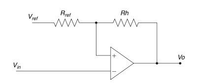
图 3.16 运放的正反馈。#
不会。为了开始分析,设 \(V_{ref} = 2.5 V\),并假设输出等于 0 V。那么 V+ 的电压是多少?你看到了——因为 Vo 等于 0,我们又得到了一个基本的分压器。假设 \(R_{ref} = 10 K\) 且 Rh = 100 K:
所以现在 V+ 为 2.275 V,而 V– 为 0 V。运放会怎么做?我们参考之前学到的运放框图——见 Figure 3.17。
图 3.17 从运放内部开始分析#
我们得到了什么?\(V_{sum}\) 等于 V+ – V–,也就是 \(V_{sum} = 2.275 V\)。Vo 等于 \(V_{sum} * G\)。显然,输出将达到正电源轨。(如果你对此不确定,请重读“什么是运放”那一节。)现在 Vo 达到正电源轨。我们假设该运放的正电源轨是 4 V。(记住,输出电压轨取决于所使用的运放,你应参考数据手册。这里使用 4 V 是基于使用 0 到 5 V 电源的 LM324 的典型值。)
输出为 4 V,V– 为 0 V,但 V+ 呢?它已经变化了。我们必须重新分析它。(你是否感觉陷入了循环?你应该有这种感觉。这就是反馈的本质;输出影响输入,输入又影响输出,如此往复。)这次分析有些不同。不能再只用分压法来计算 V+。我们必须使用“叠加原理”。
叠加原理是将一个电压源设为 0,分析其结果,再将另一个电压源设为 0,分析其结果,然后将两个结果相加,得到完整表达式。现在我们就来做这件事。我们已经知道由于 \(V_{ref}\) 带来的结果,来自之前的例子。Figure 3.18 再次展示了正反馈图。
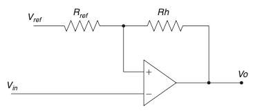
图 3.18 运放的正反馈。#
这是使用分压法计算的 \(V_{ref}\) 对 V+ 的影响结果:
这是 Vo 对 V+ 的影响结果:
两个电压源叠加的最终结果为:
现在代入所有当前值,我们得到:
这个电路现在稳定了吗?是的。V– 为 0 V,V+ 为 2.64 V。这导致了一个正误差,经过运放的开环增益放大后,使输出达到正电源轨,即我们刚才分析的 4 V 状态。
现在让我们改变一些条件看看会发生什么。开始慢慢提高 V– 的电压。当 V– 电压超过 V+ 的电压时,运放输出会发生变化。此时产生负误差,使输出跳转到负电源轨。V+ 又会变回我们上面计算的 2.275 V。那么如何让输出再次变为正?我们需要将输入调低到小于 2.275 V。正反馈会强化输出的变化,使得必须将输入进一步向相反方向移动,才会再次改变输出。
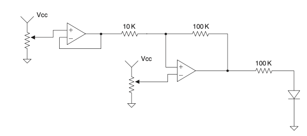
图 3.19 放在实验台上的简单运放电路,帮助你理解正反馈和负反馈。#
我刚才描述的这种效应称为“迟滞”。它是通过使用带正反馈的运放常见地实现的一种效应。“迟滞有什么用?”你可能会问。嗯,比如加热你的房子。迟滞可以防止你的炉子每几秒就开启关闭一次。你的烤箱和冰箱也使用这个原理。事实上,我写这段文字用的电脑中的硬盘也用迟滞来存储信息。
一个重要说明项:迟滞窗口的大小取决于两个电阻 \(R_{ref}\) 和 Rh 的比值。在大多数典型应用中,Rh 比 \(R_{ref}\) 大得多。如果 Vi 的信号小于窗口值,就可能创建一个电路,使输出锁定在高或低状态,且永不改变。这通常不是所期望的情况,可以通过执行上述分析并将计算得出的限制与输入信号范围进行比较来避免。
现在我们已经介绍完运放的三种基本配置,让我们构建一个结合它们的简单电路。在这里,我们有一个电压跟随器,连接到一个带迟滞的比较器,并用 LED 作为指示灯(见 Figure 3.19)。你应该在实验室中搭建这个电路,以便直观理解所讨论的内容。试验在电路各部分中改变反馈。注意你可以将输入电位器从 5K 换成 100K,而不会影响比较器切换的电压。
What is positive feedback? Let’s take a look at a real-world example. You are hard at work one day when your boss stops by and says,“Hey, you should know that you’ve handled your project very well, and that new op-amp circuit you built is awesome!” After you bask in his praise for a while, you find yourself working even harder than before. [20] This is positive feedback. The output is sent back to the positive input, which in turn causes the output to move further in the same direction. Let’s look at the op-amp diagram again—see Figure 3.16.
Now we will do a little intuitive analysis. Don’t forget the Thumb Rules we learned in the last two sections. Review them now if you need to.
Begin by applying 0 V to \(V_{in}\) . In this case the input is connected to V–. You also see that the output is connected via a resistor to a reference voltage, Vref . What is the voltage at V–? Does the voltage at V– equal the voltage at V+? No! (Don’t believe me? Check the Thumb Rules!)
What is the voltage at V+? That depends on two things: the voltage at Vref and the output voltage of the amplifier, Vo. Does the V+ input load the circuit at all?
FIGURE 3.16 Positive feedback on an op-amp.#
No, it does not. To begin the analysis, let \(V_{ref} = 2.5 V\), and assume that the
output is equal to 0 V. Now what is the voltage at V+? What do you know—since
Vo is equal to 0, we have a basic voltage divider again. Assume \(R_{ref} = 10 K\) and
Rh= 100 K:
So now there is 2.275 V at V+ and 0 V at V–. What will the op-amp do? Let’ refer to the op-amp block diagram we learned earlier—see Figure 3.17.
FIGURE 3.17 Start with what is really inside#
What do we have? \(V_{sum}\) is equal to V+ – V– or, in this case, \(V_{sum} = 2.275 V\). Vo is
equal to \(V_{sum} * G\). The output will obviously go to the positive rail. (If this is not
obvious to you, you need to review“What Is an Op-Amp, Really?” again.) Now
we have Vo at the positive rail. Let’s assume that it is 4 V for this particular
op-amp. (Remember, the output rails depend on the op-amp used, and you
should always refer to the datasheets for that information. 4 V used in this case
is typical for an LM324 with a 0 to 5 V supply.)
The output is at 4 V and V– is at 0 V, but what about V+? It has changed. We must go back and analyze it again. (Do you feel like you are going in circles? You should. That is what feedback is all about; outputs affect inputs, which affect the outputs, and so on, and so on.) The analysis this time has changed slightly. It is no longer possible to use just the voltage divider rule to calculate V+. We must also use superposition.
In superposition, you set one voltage source to 0 and analyze the results, and then you set the other source to 0 and analyze the results. Then you add the two results together to get the complete equation. Let’s do that now. We already know the result due to \(V_{ref}\) from our previous example. Figure 3.18 shows the positive feedback diagram again for reference.
FIGURE 3.18 Positive feedback on an op-amp.#
Here is the result due to \(V_{ref}\) using the voltage divider rule:
Here is the result due to Vo using the voltage divider rule:
The result due to both is thus:
Now insert all the current values and we have:
Is this circuit stable now? Yes, it is. We have 0 V at V– and 2.64 V at V+. This results in a positive error, which, when amplified by the open-loop gain of the op-amp, causes the output to go to the positive rail. This is 4 V, which is the state that we just analyzed.
Now let’s change something and see what happens. Let’s start slowly ramping up the voltage at V–. At what point will the op-amp output change? Right after the voltage at V– exceeds the voltage at V+. This results in a negative error, causing the output to swing to the negative rail. And what happens to V+? It changes back to 2.275 V, as we calculated above. So how do we get the output to go positive again? We adjust the input to less than 2.275 V. The positive feedback reinforces the change in the output, making it necessary to move the input farther in the opposite direction to affect another change in the output.
FIGURE 3.19 Simple op-amp circuit for your bench to help you understand both positive and negative feedback.#
The effect that I have just described is called hysteresis. It is an effect very commonly created using a positive feedback loop with an op-amp.“What is hysteresis good for?” you ask. Well, heating your house, for one thing. It is hysteresis that keeps your furnace from clicking on and off every few seconds. Your oven and refrigerator use this principle as well. In fact, the disk drive on the computer I used to write this paragraph uses hysteresis to store information.
One important item to note: The size of the hysteresis window depends on the ratio of the two resistors \(R_{ref}\) and Rh. In most typical applications, Rh is much larger than \(R_{ref}\) . If the signal at Vi is smaller than the window, it is possible to create a circuit that latches high or low and never changes. This is usually not desired and can be avoided by performing the preceding analysis and compar- ing the calculated limits to the input signal range.
Now that we have covered the three basic configurations of an op-amp, let’s put together a simple circuit that uses them. Here, we have a voltage follower, hooked to a comparator using hysteresis, with an LED as an indicator (Figure 3.19). You should build this in your lab to gain an intuitive understanding of what has been discussed. Experiment with feedback changes in all parts of the circuit. Note that you can change the input potentiometers from 5 to 100 K without affecting the voltage at which the comparator switches.
关于运算放大器#
All About Op-Amps
这就是运算放大器电路的基础。有了这些信息,你可以分析你遇到的大多数运放电路,并自己构建一些非常巧妙的电路。你会问,那滤波器呢?嗯,滤波器无非就是一种根据频率改变增益的放大器。只需用电容或电感替换电阻,从而为电路添加一个频率成分。
你又会问,那振荡器呢?这些是反馈电路,其中信号的时序很重要。 [21] 它们仍然遵循前面的规则。我必须再次强调:掌握任何学科的基础是你能做的最重要的事情。如果你理解了基础知识,就可以在此基础上不断深入获取更高层次的知识;但如果你“没有掌握基础”,你将在所选择的领域中徘徊不前。
经验法则
运放输入是高阻抗的(这意味着没有电流流入输入端);这一点再怎么重复都不过分,请原谅我重复说它。
运放输出是低阻抗的。
V+ = V–只有在存在负反馈时才成立;如果是正反馈,它们不需要相等。正反馈在设置得当时会产生迟滞效应。
正反馈可以使输出锁定在某一状态。
带延迟的正反馈可以引起振荡。
运放是为了简化放大设计而发明的,所以不要把它复杂化!
There you have it—the basics of op-amp circuits. With this information, you can analyze most op-amp circuits you come across and build some really neat ones yourself. What about filters, you say! Well, a filter is nothing more than an amplifier that changes gain, depending on the frequency. Simply replace the resistors with a cap or inductor and thus add a frequency component to the circuit.
What about oscillators, you say? These are feedback circuits where timing of the signals is important. [21] They still follow the preceding rules. I must reiterate my belief that grasping the basics of any discipline is the most important thing you can do. If you understand the basics, you can always build on that foundation to obtain higher knowledge, but if you do not“get the basics,” you will flounder in your chosen field.
Thumb Rules
Op-amp inputs are high impedance (that means no current flows into the inputs); this can’t be said too often, so forgive me for repeating it.
Op-amp outputs are low impedance.
V+ = V–only if negative feedback is present; they don’t have to be equal if feedback is positive.Positive feedback creates hysteresis when properly set up.
Positive feedback can make an output latch to a state and stay there.
Positive feedback with a delay can cause an oscillation.
Op-amps were designed to make it easy, so don’t make it hard!
它应该是逻辑的#
IT’S SUPPOSED TO BE LOGICAL
二进制数#
Binary Numbers
二进制数 对于电气工程来说是如此基本,以至于我差点因为你可能已经了解它们而省略本节。然而,我自己说过的“扎实掌握基础”这句话一直萦绕在我脑海中。所以,如果你对这些内容已经了如指掌,你可以跳过本节;但如果你也开始被这句话困扰,就像我希望的那样,那么你至少应该略读一下。
二进制数只是一种用两个值(1 和 0)来计数的方法——稍后我们将讨论这两个数字为何如此方便。二进制也称为基数 2。此外还有其他进制,如八进制(基数 8)和十六进制(基数 16),它们在该领域中也经常使用,主要是因为它们可以方便地表示二进制数。人们最常用的是十进制 [22],也就是基数 10。可以这样思考:一个计数系统的“基数”就是你将一位数进位到左边一列并从 0 重新开始的那个点。例如,在十进制中你从 0、1、2、3… 7、8、9 数起,然后向左进一位并从 0 重新开始,得到数字 10。在八进制中你只能数到 7,然后必须重新开始:0、1、2… 5、6、7、10、11,如此类推。十六进制也是类似地在 15 时进位,但为了满足“每列只能有一个数字”的规则,我们用字母表示 10 到 15。Table 3.1 展示了这种关系的直观表示。
表 3.1 十进制与十六进制数字
十进制(基数 10) |
十六进制(基数 16) |
0 |
0 |
1 |
1 |
2 |
2 |
3 |
3 |
4 |
4 |
5 |
5 |
6 |
6 |
7 |
7 |
8 |
8 |
9 |
9 |
10 |
A |
11 |
B |
12 |
C |
13 |
D |
And so on… |
注意这些数字如何在相应的基数下重新开始。你可能还注意到我在计数时从 0 开始。 [23] 应特别强调的是,0 是任何计数系统中都非常重要的组成部分,这一点常常被忽视。想一想,如果包括 0,十进制的进位点是第十个数字,八进制的进位点是第八个数字。对于任何使用的进制来说,都会存在相同的关系。
回到二进制或基数 2。我第一次看到二进制数时,我想:“哇,这是一种多么诱人的 [24] 数字系统;你刚刚迈出一步到达目的地,就得重新开始。”数字如下:0、1、10、11、100…… 我认为这时候表格最能说明问题——见 Table 3.2。
表 3.2 十进制、二进制、八进制和十六进制对比
十进制(基 10) |
二进制(基 2) |
八进制(基 8) |
十六进制(基 16) |
0 |
0 |
0 |
0 |
1 |
1 |
1 |
1 |
2 |
10 |
2 |
2 |
3 |
11 |
3 |
3 |
4 |
100 |
4 |
4 |
5 |
101 |
5 |
5 |
6 |
110 |
6 |
6 |
7 |
111 |
7 |
7 |
8 |
1000 |
10 |
8 |
9 |
1001 |
11 |
9 |
10 |
1010 |
12 |
A |
11 |
1011 |
13 |
B |
12 |
1100 |
14 |
C |
13 |
1101 |
15 |
D |
14 |
1110 |
16 |
E |
15 |
1111 |
17 |
F |
16 |
10000 |
20 |
10 |
17 |
10001 |
21 |
11 |
18 |
10010 |
22 |
12 |
And so on … |
表 3.3 位权重(倍增规律)
十进制 |
128 |
64 |
32 |
16 |
8 |
4 |
2 |
1 |
二进制 |
10000000 |
1000000 |
100000 |
10000 |
1000 |
100 |
10 |
1 |
注意八进制和十六进制在二进制位数增加的节点处“进位”。这正是它们在表示二进制数时非常方便的原因。你可能也注意到十进制数并不能如此整齐地对齐。
你还应在表格中发现另一个模式:你在八进制中遇到 20 的时候,刚好也是十六进制中遇到 10 的时候。这是有道理的,因为一个基数恰好是另一个的两倍。你能推测出四进制会怎样吗?
这就引出另一个关于二进制数的技巧。每个有效位的权重是前一位的两倍(就像十进制中每添加一位就是前一位的 10 倍)。我们再看一个表格——见 Table 3.3。
你可以将二进制中为 1 的位所代表的值加总起来得到其十进制值。例如,取二进制数 101。1 出现在 1 位和 4 位。1 加 4 等于 5,这就是 101 所对应的十进制数。你还会注意到,每添加一位,能表示的数值范围就会加倍。例如,四位能计数到 15,八位能计数到 255。(这导致我们这些外向的工程师在聚会时试图炫耀自己能用十个手指数到 1023——通常都以失败告终。)
你在十进制中学到的所有数学技巧在二进制中也适用,只要你考虑到你所使用的基数。
例如,在十进制中乘以 10 只是末尾加一个 0,对吧?在二进制中也一样,只是基数是 2,所以乘以 2 只需在末尾加一个 0,其它位整体左移一位。在十进制中除以 10 就是去掉末位数字并保留余数。在二进制中除以 2 也类似,整体右移一位,但余数始终是 0 或 1——这一事实对后续学习的数学运算非常方便。
出于某种原因,大多数电子元件喜欢以 4 位为单位处理二进制数。这使得十六进制(hex)成为一种表示二进制的速记方法。这是一种值得掌握的速记。在电子世界中,每个二进制位通常称为一个 bit(位),8 个 bit 称为一个 byte(字节),4 个 bit 称为一个 nibble(半字节)。所以,如果你“咬”(byte)得太多下不去,也许你下次应该“啃一口”(nibble)试试。
回到正题:由于一个十六进制数可以很好地表示一个 nibble,而一个 byte 由两个 nibble 组成,所以我们通常使用两个十六进制数来描述一个字节的二进制信息。例如,0101 1111 可以写作 5F,而 1110 0001 可以写作 E1。事实上,你只需参考 Table 3.2 就能轻松找到任何 nibble 对应的十六进制值。
总结一下,二进制数是只使用两个符号计数的方法;它们常通过十六进制作为一种速记表示方式。当逻辑电路出现时,它们只使用两个状态(开或关,高或低)来表示信息,这与二进制数和二进制运算天然契合。
Binary numbers are so basic to electrical engineering that I nearly omitted this section on the premise that you would already know about them. However, my own words,“drill the basics,” kept haunting me. So if you already know this stuff forward and backward, you are authorized to skip this section, but if those same words start to haunt you, as I hope they will, you should at least skim through it.
Binary numbers are simply a way to count with only two values, 1 and 0— convenient numbers for reasons we will discuss later. Binary is also known as base 2. There are other bases, such as base 8 (octal) and base 16 (hexadecimal), that are often used in this field, but it is primarily for the reason that they rep- resent binary numbers easily. The common base that everyone is used to is decimal, [22] also known as base 10. Think of it this way: The base of the counting system is the point at which you move a digit into the left column and start over at 0. For example, in base 10 you count 0, 1, 2, 3… 7, 8, 9 and then you chalk one up in the left column and start over at 0 for the number 10. In base 8 you only get to 7 before you have to start over: 0, 1, 2… 5, 6, 7, 10, 11, and so on. Base 16 starts over at 15 in the same way, but to adhere to the rule of one digit in the column before we roll over into the next digit, we use letters to represent 10 through 15. Table 3.1 shows an easy way to see this relationship.
Table 3.1 Decimal and Hexadecimal Numbers
Decimal, Base 10 |
Hexadecimal, Base 16 |
0 |
0 |
1 |
1 |
2 |
2 |
3 |
3 |
4 |
4 |
5 |
5 |
6 |
6 |
7 |
7 |
8 |
8 |
9 |
9 |
10 |
A |
11 |
B |
12 |
C |
13 |
D |
And so on… |
Note again how the numbers start over at the corresponding base. You might also notice that I started at 0 in the counting process. [23] It should be stressed that 0 is an important part of any counting system, a fact that I think tends to get overlooked. If you think about it, when 0 is included, the point at which base 10 rolls over is the 10th digit and the point at which base 8 rolls over is the 8th digit. The same relationship exists for any base number you use.
So, let’s get back to binary or base 2. The first time I saw binary numbers I thought,“Wow, what a tantalizing [24] numeric system; just as soon as you make one move to get where you are going, it is time to start over again.” The numbers go like this: 0, 1, 10, 11, 100…. Again, I think a table is in order—see Table 3.2.
Table 3.2 Decimal, Binary, Octal, and Hexadecimal Number Comparison
Decimal, Base 10 |
Binary, Base 2 |
Octal, Base 8 |
Hexadecimal, Base 16 |
0 |
0 |
0 |
0 |
1 |
1 |
1 |
1 |
2 |
10 |
2 |
2 |
3 |
11 |
3 |
3 |
4 |
100 |
4 |
4 |
5 |
101 |
5 |
5 |
6 |
110 |
6 |
6 |
7 |
111 |
7 |
7 |
8 |
1000 |
10 |
8 |
9 |
1001 |
11 |
9 |
10 |
1010 |
12 |
A |
11 |
1011 |
13 |
B |
12 |
1100 |
14 |
C |
13 |
1101 |
15 |
D |
14 |
1110 |
16 |
E |
15 |
1111 |
17 |
F |
16 |
10000 |
20 |
10 |
17 |
10001 |
21 |
11 |
18 |
10010 |
22 |
12 |
And so on … |
Table 3.3 Doubling Digits
Decimal |
128 |
64 |
32 |
16 |
8 |
4 |
2 |
1 |
Binary |
10000000 |
1000000 |
100000 |
10000 |
1000 |
100 |
10 |
1 |
Notice how base 8 and base 16 roll over right at the same point that the binary numbers get an extra digit. That is why they are convenient to use in representing binary numbers. You might also have noticed that decimal numbers don’t line up as nicely.
Another pattern you should see in this table is that you hit 20 in base 8 at the same point at which you see 10 in base 16. This makes sense because one base is exactly double the other. Can you extrapolate what base 4 might do? This leads to another trick with binary numbers. Each significant digit doubles the value of the previous one (just as every digit you add in decimal is worth 10 times the previous one). Let’s look at yet another table—see Table 3.3.
You can add up the values of each digit where you have a 1 in binary to get the decimal equivalent. For example, take the binary number 101. There is a 1 in the 1s column and in the 4s column. Add 1 plus 4 and you get 5, which is 101 in binary. You might also notice that the numbers you can represent double for every digit you add to the number. For example, four digits let you count to 15, and eight digits will get you to 255. (This causes some of us more extroverted engineers to attempt to become the life of the party by showing their friends that they can count to 1023 with the fingers on their hands. These attempts usually fail.)
All the math tricks you learned with decimal numbers apply to binary as well, as long as you consider the base you are working in.
For example, when you multiply by 10 in decimal, you simply put a 0 on the end, right? The same idea applies to binary, but the base is 2, so to multiply by 2, you simply stick a 0 on the end, shifting everything else to the left. When dividing by 10 in decimal you simply lop off the last digit and keep whatever was there as a remainder. Dividing by 2 in binary works the same way, shifting everything to the right, but the remainder is always 0 or 1—a fact that is convenient for math routines, as we will learn later.
For whatever reason, most electronic components like to manage binary num- bers in groups of four digits. This makes hexadecimal (or hex) numbers a type of shorthand for referring to binary numbers. It is a good shorthand to know. In the electronics world, each binary digit is commonly referred to as a bit. A group of eight bits is called a byte and four bits is called a nibble. So if you“byte” off more than you can chew, maybe you should try a“nibble” next time.
Back to the point: Since a hex number nicely represents a nibble, and there are two nibbles in a byte, you will often see two hex numbers used to describe a byte of binary information. For example, 0101 1111 can be described as 5 F or 1110 0001 as E 1. In fact, you can easily determine this by looking up the hex equivalent to any nibble using Table 3.2.
To sum things up, binary numbers are a way to count using only two symbols; they are commonly referred to using hex numbers as a type of shorthand nota- tion. When logic circuits came along, the fact that they represented information with only two symbols—on or off, high or low—made them dovetail nicely with binary numbers and binary math.
逻辑#
Logic
在过去的 50 年中,最令人难以置信的增长产业之一源于将电子技术应用于基于布尔逻辑原理的数据处理。布尔逻辑最初由 George Boole 在 19 世纪中叶提出,其基础概念非常简单,却能够构建出非常复杂的系统。
让值 1 表示“真”,值 0 表示“假”。在实际电路中,1 通常表示介于 3 到 5 伏之间的信号,而 0 通常表示 0 到 2.9 伏之间的信号,但在逻辑领域,重要的是状态只有两种:1 或 0。这个世界要么是黑,要么是白。正因为如此,工程师们才能如此迅速地掌握数字领域。我还没遇到过哪位工程师不喜欢他的世界遵循清晰可预见的规则。“保持简单”是一句常听的口头禅,将世界简化为两种状态确实可以简化很多问题。值得注意的是,在某个电路的节点上必须做出判断:当前值究竟代表 1 还是 0。
在学习逻辑的过程中,我们会参考一种描述逻辑输入输出关系的方法,称为“真值表”。在这些表中,输入通常在左边,输出在右边。一些用于处理逻辑的基本元件被称为“门”。我们从这些基础内容开始。
One of the most incredible growth industries over the last 50 years has come from the application of electronics to manipulate data based on the principles of Boolean logic. Originally developed by George Boole in the mid-1800s, Boo- lean logic is based on a very simple concept yet allows creation of some very complex stuff.
Let the value 1 mean true, and let the value 0 mean false. In an actual circuit, 1 might typically be any signal between 3 to 5 V, and 0 any signal between 0 to 2.9 V, but what is important in the world of logic is that there are only two states, 1 or 0. The world is black or white. That said, it is no wonder that engineers have so quickly grasped the digital domain. I haven’t met an engineer who doesn’t like his world to follow nice, predictable rules.“Keep it simple” is a common mantra, and resolving the world into two states sure does simplify things. It is important to note that at some point in the circuit a decision needs to be made whether the current value represents a 1 or a 0.
During our study of logic we will refer to a description of logic inputs and out- puts known as truth tables. In these tables, the inputs are generally shown on the left and the outputs are on the right. Some basic components that manipulate logic are called gates. Let’s start with these basics.
非门(NOT)#
The NOT Gate
这是最简单的逻辑门。非门会反转你输入的任何信号;输入 1,输出 0;输入 0,输出 1。我们可以用晶体管构建一个非门,如 Figure 3.20 所示。
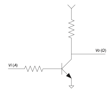
图 3.20 晶体管非门。#
如果你向其输入 0 伏,将得到 5 伏输出;如果输入 5 伏,将得到几乎为 [25] 0 伏的输出。你实际上反转了逻辑状态。非门,也称为反相器,常用的符号如 Figure 3.21 所示。Table 3.4 展示了它的真值表。 [26]
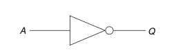
图 3.21 非门或反相器的符号。#
表 3.4 非门真值表
输入 A |
输出 Q |
1 |
0 |
0 |
1 |
This is as simple as it gets. The NOT gate inverts whatever signal you put into it; put in a 1, get a 0 out, and vice versa. Let’s take a transistor and make a NOT gate, as shown in Figure 3.20.
FIGURE 3.20 Transistor NOT gate.#
If you put 0 V into this, you will get 5 V out. If you put 5 V into this, you will get nearly [25] 0 V out. You have effectively inverted the logic symbol. The NOT gate, also called the inverter, is commonly represented by the symbol shown in Figure 3.21. Table 3.4 shows the truth table. [26]
FIGURE 3.21 Inverter or NOT symbol.
Table 3.4 NOT Gate Truth Table
Input A |
Output Q |
1 |
0 |
0 |
1 |
与门(AND)#
The AND Gate
与运算的规则是:只有所有输入都为真(1),输出才为真。也就是说,如果这个条件为真,并且那个条件也为真,那么“这个 AND 那个”才为真。但只要有一个为假,输出就必须为假。真值表如 Table 3.5 所示。
表 3.5 与门真值表
输入 A |
输入 B |
输出 Q |
0 |
0 |
0 |
0 |
1 |
0 |
1 |
0 |
0 |
1 |
1 |
1 |
我们可以只用几个二极管构建这个电路。换一种方式理解:只要有一个输入为假,输出就是假——参见 Figure 3.22。该功能常用的符号如 Figure 3.23 所示。
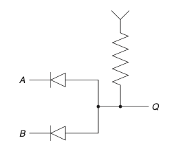
图 3.22 二极管实现的与门。#
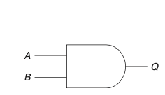
图 3.23 与门符号。#
The AND function is described by the rule that all inputs need to be true or 1 in order for the output to be true. If this is true and that is true, this AND that must be true. However, if either is false, the output must be false. It is defined by the truth table shown in Table 3.5.
Table 3.5 AND Gate Truth Table
Input A |
Input B |
Output Q |
0 |
0 |
0 |
0 |
1 |
0 |
1 |
0 |
0 |
1 |
1 |
1 |
We can build this circuit with only a couple of diodes. One way to think of it is that if either input is false, the output will be false—see Figure 3.22. This function is commonly referred to by the symbol in Figure 3.23.
FIGURE 3.22 Diode AND gate.#
FIGURE 3.23 AND gate.#
或门(OR)#
The OR Gate
你有没有注意到,与门中有三种输入条件会导致输出为假(0)?而或门则有点相反,但也不完全相反。有三种输入条件会使输出为真,只有一种情况输出为 0。换句话说,只要“这个为真”或“那个为真”,输出就为真。真值表见 Table 3.6。
表 3.6 或门真值表
输入 A |
输入 B |
输出 Q |
0 |
0 |
0 |
0 |
1 |
1 |
1 |
0 |
1 |
1 |
1 |
1 |
我们也可以使用二极管构建这个电路,只是将它们反向放置,如 Figure 3.24 所示。更常用的或门符号如 Figure 3.25 所示。
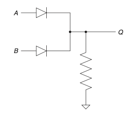
图 3.24 二极管实现的或门。#
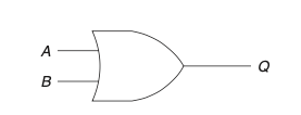
图 3.25 常见的或门符号。#
就这样——这些就是最基本的逻辑门。一共只有三个。“等一下,”你可能会说,“我在上逻辑电路课的时候明明见过更多种门电路!”确实还有更多门电路,但它们全都是由这三种基本门构成的。如果你理解了这些,就可以推导出其他逻辑门。因此,请试试看,能否仅用前述三种基本器件构建其他逻辑门。
Did you notice that three of the input conditions on the AND gate resulted in a false, or 0, at the output? The OR gate is sort of the opposite, but not exactly. Three of the input conditions result in a true at the output, whereas only one condition creates a 0. If this is true OR that is true, it only takes one true input to create a true output. \(Table 3.6 <Table 3.6>\) shows the truth table.
Table 3.6 OR Gate Truth Table
Input A |
Input B |
Output Q |
0 |
0 |
0 |
0 |
1 |
1 |
1 |
0 |
1 |
1 |
1 |
1 |
We can make this circuit with diodes, too; we just flip them around, as in Figure 3.24. The more common OR symbol looks like the one shown in Figure 3.25.
FIGURE 3.24 Diode OR gate.#
FIGURE 3.25 Most common OR symbol.#
That’s it—those are the basic gates. There are only three of them.“Now wait a minute,” you may be saying, there were a lot more when I had logic circuits in class, weren’t there? There are more gates, but they are all built from these three basic gates. If you understand these, you can derive the rest. With that in mind, see if you can make these other logic gates using only the previous three components.
非与门#
The NAND gate
NAND 意思是“非与”(NOT AND),它就是字面上的意思。将一个与门(AND gate)的输出通过非门(NOT gate)反转,就得到了一个 NAND 门。 表 3.7 显示了它的真值表。
表 3.7 NAND 门真值表
输入 A |
输入 B |
输出 Q |
0 |
0 |
1 |
0 |
1 |
1 |
1 |
0 |
1 |
1 |
1 |
0 |
我们可以用前面学过的基本符号构建一个 NAND 门,如 Figure 3.26 所示。这个门使用非常广泛,因此有它自己专用的符号。注意输出端的小圆圈,用来表示反转的信号。
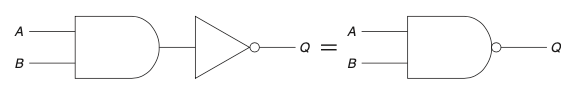
图 3.26 如何构建一个 NAND 门。#
我们是否也能使用基本的半导体器件来实现这个门呢?答案是肯定的。实际上,你只需要两个晶体管——参见 Figure 3.27。
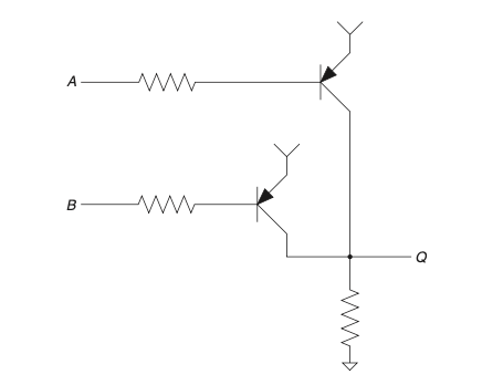
图 3.27 简单的晶体管 NAND 门。#
NAND means NOT AND, and it is what it says. Invert the output of an AND gate with the NOT gate and you have a NAND gate. Table 3.7 shows the truth table.
Table 3.7 NAND Gate Truth Table
Input A |
Input B |
Output Q |
0 |
0 |
1 |
0 |
1 |
1 |
1 |
0 |
1 |
1 |
1 |
0 |
Let’s build one with the basic symbols we have already learned, as shown in Figure 3.26. This gate is so commonly used that it has its own symbol. Note the little bubble on the output, which is used to indicate an inverted signal.
FIGURE 3.26 How to build a NAND gate.#
Can you make this gate with basic semiconductors as well? The answer is yes. In fact, you only need two transistors—see Figure 3.27.
FIGURE 3.27 Simple transistor NAND gate.#
非或门#
The NOR Gate
没错,你猜对了,这是“非或”门(NOT OR)。它是通过反转或门的输出得到的,原理和 NAND 门一样。Table 3.8 显示了它的真值表。NOR 门是反转输出的或门,其符号如 Figure 3.28 所示。更妙的是,如图 3.29 所示,你也可以只用两个晶体管构建这个门。
表 3.8 NOR 门真值表
输入 A |
输入 B |
输出 Q |
0 |
0 |
1 |
0 |
1 |
0 |
1 |
0 |
0 |
1 |
1 |
0 |
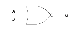
图 3.28 NOR 门符号。#
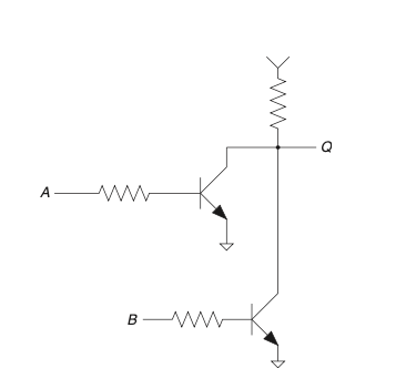
图 3.29 晶体管 NOR 门。#
Yep, you guessed it, this is the NOT OR gate. It is made by inverting the output of the OR gate, just like the NAND gate. Table 3.8 shows the truth table. The NOR gate is an inverted OR gate with a symbol like the one shown in Figure 3.28. Better yet, as Figure 3.29 shows, you can make this gate with only two transistors as well.
Table 3.8 NOR Gate Truth Table
Input A |
Input B |
Output Q |
0 |
0 |
1 |
0 |
1 |
0 |
1 |
0 |
0 |
1 |
1 |
0 |
FIGURE 3.28 NOR gate symbol.#
FIGURE 3.29 Transistor NOR gate.#
异或门(XOR)#
The XOR Gate
XOR 意思是“异或”(exclusive or)——参见图 3.30。换句话说,你可以这样理解:如果“这个”为真或“那个”为真,但不是两个都为真,则结果为真。Table 3.9 显示了它的真值表。
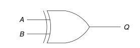
图 3.30 异或(XOR)门。#
表 3.9 XOR 门真值表
输入 A |
输入 B |
输出 Q |
0 |
0 |
0 |
0 |
1 |
1 |
1 |
0 |
1 |
1 |
1 |
0 |
让我们看看是否也能用基本的半导体元件实现这个门,就像我们对其他逻辑电路所做的那样,如 Figure 3.31 所示。
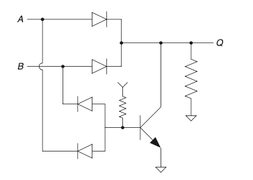
图 3.31 基于二极管和晶体管的 XOR 门。#
XNOR 门如 Figure 3.32 所示。如果我之前的解释足够清晰,你应该能够立即理解这个门的功能。它就是带有反转输出的 XOR 门。Table 3.10 显示了其真值表。
图 3.32 XNOR 门。#
表 3.10 XNOR 门真值表
输入 A |
输入 B |
输出 Q |
0 |
0 |
1 |
0 |
1 |
0 |
1 |
0 |
0 |
1 |
1 |
1 |
XOR means exclusive or—see Figure 3.30. In other words, think of it like this: It’ s true if this or that is true, but not if both are true. Table 3.9 shows the truth table.
FIGURE 3.30 XOR (exclusive OR) gate.#
Table 3.9 XOR Gate Truth Table
Input A |
Input B |
Output Q |
0 |
0 |
0 |
0 |
1 |
1 |
1 |
0 |
1 |
1 |
1 |
0 |
Let’s see whether we can make this with basic semiconductor components the same as we did with the other logic circuits, as shown in Figure 3.31.
FIGURE 3.31 Diode- and transistor-based XOR gate.#
The XNOR gate looks like the one in Figure 3.32. If I have done a good job with my explanations, the function of this gate should be obvious. It is an XOR with an inverted output. Table 3.10 shows its truth table.
FIGURE 3.32 The XNOR gate.#
Table 3.10 XNOR Gate Truth Table
Input A |
Input B |
Output Q |
0 |
0 |
1 |
0 |
1 |
0 |
1 |
0 |
0 |
1 |
1 |
1 |
加法器#
Adders
如你所知,我们可以使用这些无处不在的 1 和 0 进行计数。计数的逻辑延伸就是数学!将多个这种门组合起来,我们就可以构建一个二进制加法器;将多个加法器串联起来,就可以实现任意长度的二进制数相加。而由于任何数字都可以用一串讨厌的 1 和 0 表示,我们现在就有了计算的基础。你是否开始理解你桌上的那个计算器 [27] 是如何工作的了?
As you already know, it is possible to count with these ubiquitous 1s and 0s. The logical extension of counting is math! Joining several of these gates together, we can create a binary adder; string a bunch of these adders together to add any number of binary digits and, since any number can be represented by a string of those pesky 1s and 0s, we now have the basis of computation. Are you beginning to see how that calculator [27] on your desk works?
存储单元#
Memory Cells
我们可以使用这些器件创建所谓的存储单元。Figure 3.33 展示了其中一个的示意图。
基本原理是,这个单元会保留你设置的状态。一些存储器在断电后会丢失所存储的数据;这类存储器被称为易失性存储器。这就像你电脑中的 RAM。另一类存储器被称为非易失性存储器。这种类型在断电后依然能保留数据。一个例子就是闪存,在如今随处可见的 U 盘中就有使用。
现在你已经具备了做出决策、进行数学运算并记住结果以便后续再次使用的能力,你就掌握了图灵机的基本原理。艾伦·图灵是一位密码学家,他奠定了计算理论的基础。他描述的图灵机是一种具备无限内存、能在内存中前后移动并能在任意位置执行指令的系统。除了无限内存以外,如今的计算机已经非常接近图灵机了。
图 3.33 基于 NAND 的存储单元。#
从最初的简单逻辑门到超级计算机,越来越复杂的系统都是建立在这些简单的逻辑元件之上的。难怪每一个新一代超级酷的处理器里都拥有无数个晶体管。然而,这里还有一种“中间型”器件值得一提,因为它能帮助你理解这样一个简单器件能制造的复杂性。它被称为状态机。
It is possible to use these devices to create what is called a memory cell. Figure 3.33 presents a diagram of one.
The basic premise is that the cell will retain the state you set it to. Some mem- ory will lose the data that was stored if power is lost; this is known as volatile memory. This is like the RAM in your computer. Another category of memory is known as nonvolatile memory. In this type the data is retained even when power is removed. An example of this is Flash memory, commonly found in the now-ubiquitous thumb drive.
Now that you have the ability to make a decision, compute mathematical functions, and remember the results so you can make more decisions later, you have the basics of a Turing machine. Alan Turing was a cryptographer who laid much of the foundation for computational theory. He described the Turing machine, a system that has an infinite amount of memory, the ability to go back and forth along that memory, and the capability to follow the instructions at any location. Aside from infinite memory, today’s computers are as close as anything comes to a Turing machine.
FIGURE 3.33 NAND-based memory cell.#
From the simple gates that started it all to supercomputers, ever more complex systems are based on these simple logic components. It is no wonder that every new mega-cool processor has a gazillion transistors in it. There is a sort of“in-between” device that is worth mentioning, though, since it will help you grasp the complexities such a simple device can create. It is known as a state machine.
状态机#
State machines
状态机处于离散逻辑与微控制器之间的领域。它们通常包含某种类型的时钟、内存和大多数微控制器所具备的基本部件;不过,它们并不需要所有这些部件就能运行。
顾名思义,状态机的输出是某一时刻输入“状态”的函数。通常会使用某种时钟信号来决定何时对这些输入进行评估。存储单元,也叫做触发器,用来存储信息。触发器在时钟信号出现的那一刻反映输入的状态。因此,用于评估的条件可以存储在内存中。
逻辑元件的输入可在时钟信号的三个不同时间点被检测:下降沿、上升沿或电平检测。具体使用哪一种取决于器件本身;你需要查阅那个所有知识的来源——数据手册。
这些术语都很直观:数据在时钟信号上升、下降或保持某电平时被评估。这使得信号的时序变得非常重要。随着我们深入研究微控制器(它们本质上就是带有指令集的高级状态机),时序的重要性还将再次出现。
由于微控制器成本的下降,我相信如今纯粹由逻辑门实现的状态机已逐渐被淘汰。当它们出现时,通常是在可编程逻辑器件(PLD)中。焊接一堆 D 触发器到电路板上然后用导线包绕电路的日子已经一去不复返了。 [28] 现在连 PLD 也内置有 MCU 内核,供一般计算需求使用。
总之,布尔逻辑是所有数字技术的基础。它是一个相对简单的概念,却可以实现极其复杂的功能。我们的世界显然正迅速走向数字化。你上一次看到某个最新产品被宣传为最酷的“模拟”技术是什么时候?
State machines lie in the realm between discrete logic and microcontrollers. They usually have a clock of some type, memory, and most of the basic parts a micro has; however, they don’t need all these parts to operate.
As the name implies, the output of a state machine is a function of the“state” of the inputs at any given moment in time. Often a clock signal of some type is used to determine the moment that these inputs should be evaluated. Memory cells, also called flip-flops, are used to store information. A flip-flop reflects the state of the input at the time a clock signal was present. Thus conditions used for evaluation can be stored in memory.
The inputs of a logic element can be detected at three different points in time on the clock signal, falling edge, rising edge, or level detect. The one that is used depends on the part itself; you will need to check that source of all knowledge, the datasheet.
These terms are self-explanatory: Data is assessed when the clock signal rises, falls, or remains level. This makes the timing of the signals important. This importance of timing will come up again as we explore microcontrollers (which are really just hopped-up state machines with a defined group of instructions, but more on that later).
Due to the falling cost of microcontrollers, I believe that purely implemented state machines are going out of fashion these days. When they do appear, they are usually in a programmable logic device, also called a PLD. Gone are the days of soldering a slew of D flip-flops onto a board and wire-wrapping a circuit together. [28] Even PLDs now have an MCU core that you can cram in there for general computing needs.
In conclusion, Boolean logic is the foundation of all things digital. It is a relatively simple concept that can do some very complex things. Ours is clearly becoming a digital world. When was the last time you saw the latest widget marketed as the coolest new“analog” technology?
拇指法则(Thumb Rules)
每增加一个有效的二进制位,其数值是前一位的两倍。
比特(bit)是只有两种状态(1 或 0)的最小信息单位。
一个 nibble 有 4 位,一个字节(byte)有 8 位。
1 代表真,0 代表假。
永远查看真值表。
在电路中,某一时刻信号会被判定为高电平(1)或低电平(0);这个判定取决于器件的阈值。
设置复杂逻辑电路时,时序至关重要。
Every significant digit you add in binary doubles the value of the previous digit.
A bit is a single piece of information with only two states, 1 or 0.
There are 4 bits to a nibble and 8 bits to a byte.
1 is true, 0 is false.
Always look at the truth table.
At some point in the circuit, a signal is considered either high, 1, or low, 0; what it is depends on the thresholds of the part.
Timing is very important in setting up more complex logic circuits.
微处理器 / 微控制器基础#
MICROPROCESSOR/MICROCONTROLLER BASICS
这是电子工业中变化最快的领域之一。如今你可以以 25 美分的价格买到带有几个引脚、少量内存的微控制器,也可以花多几块钱买到几年前还被称为超级计算机的高端嵌入式处理器。所有这些都来源于我们前面讨论的少数几类半导体器件。我不会尝试去介绍具体的处理器,因为关于特定微控制器的理解已经有成堆的图书可供参考。相反,我将尝试讲解一些普遍适用的基本规则。
将一堆逻辑门组合起来,加上一些加法器、指令解码器和存储单元。把它们连接到一些输入/输出引脚上,接入时钟源,你就得到了一个微控制器或微处理器。
这两种器件非常相似,因此它们的名称经常被互换使用。不过一般来说,微控制器更加“全包”,它包含了运行所需的所有部件,都集成在一块芯片上,通常使其更专用一些(但也不多)。相比之下,微处理器需要外部内存和接口设备才能运行。这使得它更具开放性,例如在不更换芯片的情况下可以升级内存。随着这一技术领域的发展,这两种器件之间的界限已变得相当模糊。因此,在设计中充分利用这些器件所需的理念也大体相同。
This is one of the most rapidly changing fields in the electronics industry. You can purchase microcontrollers today with only six pins with just a few lines of memory at a cost of 25 cents and for just a few bucks more, high-end embedded processors that just a few years ago would have been labeled super- computers. All this from the few semiconductor types we have discussed. I will not try to cover specific processors since there are libraries of books dedicated to understanding particular micros. Instead, I will try to cover some fundamen- tal rules that can be applied in general.
Add a bunch of logic gates together and mix with some adders, instruction decoders, and memory cells. Hook it all up to some input/output pins, apply a clock source, and you get a microcontroller or microprocessor.
These two devices are very similar, and you will hear the names used some-what interchangeably. Generally, however, the microcontroller is more all inclusive, with all the elements it needs to operate included in one piece of silicon, typically making them a little (but not much) more specialized. The microprocessor by contrast needs external memory and interface devices to operate. This makes it more open ended, allowing memory upgrades without changing the chip, for example. As this area of technology has progressed, the line of distinction between these two components has blurred considerably. Hence, much of the design philosophy needed to make the most of these devices is the same.
微控制器内部有什么?#
What’s Inside a Micro?
这也许看起来像魔法,但微控制器内部的全部结构实际上就是大量的晶体管。这些晶体管构成逻辑门,而逻辑门则构成逻辑机器。我们来回顾一下微控制器内部的一些部分。
- INSTRUCTION MEMORY
我原本会称指令存储器为 ROM,即只读存储器,但如今很多微控制器可以写入自己的指令存储器。这可以是可编程存储器、硬编码的、Flash,甚至是一个外部芯片,微控制器的核心从中读取指令。这些指令以数字比特(1 和 0)形式存储,形成表示指令的字节。
- DATABUS
数据总线是微控制器的主干,是内部连接,使微控制器的各个部分能够内部通信。几乎所有在微控制器中发生的操作,都会在某个阶段通过数据总线传输。
- INSTRUCTION DECODER
指令解码器是逻辑类型电路之一。它负责解释当前的指令,并触发相应的操作任务。
- REGISTERS
寄存器是用于存储数据的地方;它们就是我们之前讨论的存储单元。这是微控制器中的 RAM,用于处理数据的临时区域。在某些情况下,它也可以是外部芯片上的存储单元。
- ACCUMULATOR
累加器是一种特殊寄存器,通常直接连接到算术逻辑单元(ALU)。当对累加器中的某个数据执行数学运算后,结果会保留在累加器中,因此被称为累加器。在很多新型微控制器中,几乎任何寄存器都可以以类似方式使用。
- ALU
算术逻辑单元,简称 ALU,是可以对数据执行各种数学和逻辑运算的部件。
- PROGRAM COUNTER
程序计数器用于追踪微控制器当前在程序中的位置。如果每个存储单元是一个带有编号的纸张,那么程序计数器就是负责追踪当前纸张编号的部件。它用于索引或寻址当前所在位置。
- TIMER COUNTERS
定时计数器用于为代码运行创建结构。有时被称为实时时钟计数器(RTCC),它们通常可以从一个独立的源运行。它们会以你设置的时间间隔“滴答”运行,不需要其他干预。有时它们可以连接到外部时钟源或输入信号。通常可以设置为在预定时间产生中断。
- INTERRUPT
中断并不是微控制器中的一个具体硬件部件,但它足够重要,值得单独说明。中断是一种监控电路,如果被触发,会让微控制器停止当前操作,转而执行与中断相关的一段代码。这些信号可以由内部状态或外部输入产生。通常只有特定引脚可以驱动中断。
- MNEMONICS AND ASSEMBLERS
我们人类不像机器那样能记住无穷无尽的二进制数据流。甚至要记住一个微控制器所有的十六进制代码都很困难。因此助记符应运而生。助记符只是表示实际存储在指令存储器中的二进制数据的代码词。
汇编器会将这些代码词转换为实际数据,生成一个文件,该文件随后被写入指令存储器。这与用于计算机的编译器略有不同。编译器会将一种代码语言(如 C)转换为在计算机上运行的代码。然而,编译器会自动处理诸如内存寻址等任务,而汇编器不会。因此,这些语言被称为高级语言。汇编语言则直接与芯片连接的硬件交互。
如今许多微控制器都有 C 汇编器,让你可以使用熟悉的语言为微控制器编写代码。但使用这种方式要小心,因为可能会因此损失许多效率。我知道有一个案例,用一个只有 4 K 内存的微控制器来控制电动牙刷。使用 C 语言的开发人员不断要求更大的微控制器,因为他们的代码装不进去。后来换成汇编语言,整个程序只用了大约 500 字节的代码。这当然是个极端案例,我相信也有很多使用 C 写出的高效设计。关键是要知道你的代码在被转换成什么。
It might seem like magic, but all that is inside a microcontroller is a whole lot of transistors. The transistors form gates, and the gates form logic machines. Let’s go over some of the parts that are in a micro.
- INSTRUCTION MEMORY
I would call instruction memory ROM, or read-only memory, but these days there are a lot of micros that can write to their own instruction memory. This can be programmable memory, hard coded, Flash, or even an external chip that the core reads to get its instructions. The instructions are stored as digital bits, 1s and 0s, that form bytes that represent instructions.
- DATABUS
The databus is the backbone of the micro, the internal connections that allow different parts of the micro to connect internally. Virtually everything that happens inside a micro will at some point move through the databus.
- INSTRUCTION DECODER
An instruction decoder is one of those logic-type circuits. It interprets the instruction that is presented and sets the corresponding tasks into motion.
- REGISTERS
Registers are places to store data; they are literally the memory cells that we discussed earlier. This is the RAM inside the micro. It is the scratch pad for manipulating data. It can also be accessed on an external chip in some cases.
- ACCUMULATOR
An accumulator is a type of special register that usually connects directly to the arithmetic logic unit (ALU). When a math function is performed on a piece of data in the accumulator, the answer is left in the accumulator; hence it accumulates the data. On a lot of the newer micros, nearly any register can be used in a similar manner.
- ALU
The arithmetic logic unit, or ALU, is a part that can perform various mathematical and logic operations on a piece of data.
- PROGRAM COUNTER
The program counter keeps track of where the micro is in its program. If each piece of memory were a sheet of paper with a number on it, the program counter is the part that keeps track of the number on the sheets. It indexes or addresses which sheet it is on.
- TIMER COUNTERS
Timer counters are useful for creating a structure for your code to operate in. Sometimes called real-time clock counters (RTCC), they are counters that usually can run from an independent source. They will“tick” at whatever interval you set them up to tick, without any other intervention. Sometimes they can be hooked up to external clock sources and inputs. Usually they can be set to generate an interrupt at a preset time.
- INTERRUPT
Not exactly a specific hardware component in a micro, the interrupt is so important that it warrants mention. An interrupt is a monitoring circuit that, if triggered, makes the micro stop what it is doing and execute a piece of code associated with the interrupt. These signals can be generated by internal conditions or external inputs. Typically only certain pins can drive interrupts.
- MNEMONICS AND ASSEMBLERS
We humans, unlike machines, have a tough time remembering endless streams of binary data. Even trying to remember all the hex codes for a micro is very dif ficult. For this reason mnemonics were invented. Mnemonics are nothing more than code words for the actual binary data stored in the instruction memory.
An assembler takes these code words and changes them to the actual data, creat- ing a file that is then copied into the instruction memory. This differs somewhat from compilers used to compile code that you write for a computer. The compi- ler takes a code language such as C, for example, and creates code that will run on the computer. However, the compiler will handle tasks such as addressing mem- ory without any need for you to worry about it, unlike an assembler. This is why they are called higher-level languages. Assembly language, as it is called, works directly with the hardware that the chip is hooked up to.
There are a lot of micros these days that have C assemblers, allowing you to use a language you are familiar with to write code for your micro. However, use caution with this approach. It is possible to lose a lot of efficiency this way. I know of one case where a micro with 4 K of memory was being used to con- trol an electric toothbrush. The developers coding in C kept coming back for micros with more memory because they couldn’t get their code to fit. Once it was written in assembly, the whole thing took about 500 bytes of code. This is an extreme case. I’m sure there are much more efficient designs out there using C. Just be sure you have an idea of what your code is turning into.
结构#
Structure
你可以用无限种方式来组织你的代码结构。以下是一些我希望在有人把芯片和应用手册交给我之前就能学到的基本方法论。
大多数微控制器一次只做一件事。 [29] 当然,它们的运行速度非常快,以至于看起来像是在执行多任务,但事实是,每一条指令执行时,实际上只做了一件事情。这意味着时序结构对设计效率会有巨大影响。
考虑一个简单的问题。你设计了一个程序,每秒检查一次某个输入引脚。以下是其中一种实现方式(注意使用的是“darrencode”,一种强大而直观的编码工具。可惜它不支持任何已知微控制器):
Initialization

Clear counters

Setup I/O

Sense input

    Read pin

    Store reading

Delay loop

    Do nothing for 1 microsecond

    Jump to Delay loop 100,000 times

Delay done

    Jump to Sense input
这种方法存在一个小问题,你可能已经注意到了。处理器整个时间都在等待下次输入,什么都没干。如果你不打算让芯片执行其他任务,这种方式还可以接受。但如果你想更充分利用微控制器的能力,就需要想办法让它在等待期间也能做点别的事情,然后在正确时间返回去检查输入。最好的办法是使用定时中断。
中断就是其字面意思。想象你有个助手,你告诉他盯着钟表,在下午 5 点之前提醒你去开一个重要会议。你正忙着工作时,你的助手进来打断你,提醒你该走了。如果你像这些芯片一样准时,你就会立刻放下手头的事去处理紧急任务,处理完后再返回继续刚才的工作。在微控制器术语中,这叫做处理中断。
大多数微控制器都有一个由主时钟驱动的定时器,可以设置为定期触发中断。我们来看下用中断时序解决上面问题的方案:
Initialization

Setup Timer Interrupt to trigger every 1 microsecond

Clear counters

Setup I/O

Main loop

    Calculate really fast stuff

Tenth second loop

    Check tenth second flag

    Jump to End tenth if not set

    Do more tasks

    Call some routines

    End tenth

Second loop

    Check second flag

    Jump to End second if not set

    Read pin

    Store reading

End second

    Jump to Main loop

Timer Interrupt

    Increment microsecond counter

    If microsecond count equals 10,000

        set tenth second flag

        increment tenth counter

        clear microsecond count

    Else clear microsecond flag

If tenth count equals 10

    set second flag

    clear tenth count

end interrupt
需要注意的是,你不应该在中断中加入过多的任务。如果中断里包含的内容太多,可能会出现“溢出”问题,也就是中断频繁得让你什么都干不了。(我相信你肯定遇到过让你充分理解这种感觉的老板。)在 darrencode 示例中,中断中唯一的操作就是增加计数器和设置标志。所有基于时间的任务都会在主循环中,当检测到对应标志被设置时执行。
妙的是,如今我们有了一个结构,可以在需要时读取输入,同时还能腾出时间做别的事情,比如分析这个输入意味着什么、该做出什么反应。这种结构其实就是一个简易操作系统。就我个人而言,我喜欢叫它 darrenOS。你可以在你下一个微控制器项目中,自由地把你的名字加在 O 和 S 前面,形成自己的定时系统名称。(在此输入你的名字)OS 是一个自由命名领域,我保证你不会从中遇到任何间谍软件!
我认为这种结构最大的缺点,是理解其工作方式所需的复杂性。第一个示例很直观,但你一旦走进第二个示例的代码,可能就会觉得难以理解。这会导致你的代码中出现 bug,仅仅是因为更难追踪逻辑结构。如果你不打算让微控制器执行其他任务,第一个示例完全没有问题。然而,第二种结构的时序方案最终更具灵活性与强大功能。这里的权衡是:简单性与受限功能 VS 复杂性与更高的微控制器利用率。
有编程经验的你可能会问:“为什么不直接把输入引脚连到中断上,只在其发生变化时再去检查?”这是个好问题。有些情况下,这种中断驱动的 I/O 方法是完全合理的,比如当你需要对该输入做出极快响应时。然而,在任何一种微控制器中,你能使用的中断资源都是有限的。如果你对每个 I/O 引脚都这样做,很快你就用完了所有中断资源。该结构的另一个好处是,它能够自然过滤掉输入引脚连接到外部世界时可能出现的噪声或信号抖动。
The various ways you can structure your code are as infinite as numbers themselves. There are some basic methodologies that I wish I had been taught before someone handed me a chip and an application note in the lab.
Most microcontrollers only do one thing at a time. [29] Granted, they can do things very fast so as to appear to be multitasking, but the fact is, at each specific instruction only one thing is being accomplished. What this means is that timing structure can have a huge effect on the efficiency of a design.
Consider this simple problem. You have a design where you need to look at an input pin once per second. One way of doing this is as follows (note the use of “darrencode,” a powerful and intuitive coding tool. Too bad it doesn’t run on any known micro!):
Initialization

Clear counters

Setup I/O

Sense input

    Read pin

    Store reading

Delay loop

    Do nothing for 1 microsecond

    Jump to Delay loop 100,000 times

Delay done

    Jump to Sense input
There is a slight problem with this method that you might have already noticed. The processor spent the whole time waiting for the next input, doing nothing. This is fine if you don’t need the chip to do anything else. However, if you want to get the most out of your micro, you need to find a way to make it do some- thing else while you wait and come back to the input at the right time. The best way to do this is with timing interrupts.
An interrupt is just what it says. Imagine you have an assistant that you have told to watch the clock and remind you right before 5:00 p.m. that you need to go to that important meeting. You are hard at work when your assistant walks in and interrupts you to let you know it is time to go. Now if you are as punctual as one of these chips, you drop whatever you are doing and go take care of business, coming back to your task at hand after you have taken care of the interruption. In micro terms this is known as servicing the interrupt.
Most micros have a timer that runs off the main clock, which can be set to trig- ger an interrupt every so often. Let’s solve the previous problem using interrupt timing and see how it looks:
Initialization

Setup Timer Interrupt to trigger every 1 microsecond

Clear counters

Setup I/O

Main loop

    Calculate really fast stuff

Tenth second loop

    Check tenth second flag

    Jump to End tenth if not set

    Do more tasks

    Call some routines

    End tenth

Second loop

    Check second flag

    Jump to End second if not set

    Read pin

    Store reading

End second

    Jump to Main loop

Timer Interrupt

    Increment microsecond counter

    If microsecond count equals 10,000

        set tenth second flag

        increment tenth counter

        clear microsecond count

    Else clear microsecond flag

If tenth count equals 10

    set second flag

    clear tenth count

end interrupt
One thing to note is that you don’t want to put a lot of stuff to do inside the interrupt. If you put too much in there you can have a problem known as over- flow, where you are getting interrupted so much that you never get anything done. (I’m sure you have had a boss or two who helped you understand exactly how that feels.) In the darrencode example, the only thing that happens in the interrupt is incrementing counters and setting flags. Everything that needs to happen on a timed base is done in the main loop whenever the corresponding flag is set.
The cool thing is that now we have a structure that can read the input when you need it to and still have time to do other things, such as figure out what that input means and what needs to be done about it. This structure is a rudimentary operating system. In my case, I like to call it darrenOS. Feel free to insert your name in front of a capital O and S for the timed code you create on your next micro. (Insert your name here) OS is a free domain, and I promise you won’t get any spyware using it!
The biggest downside to this type of structure, in my opinion, is the added complexity in understanding how it works. The first example is straightforward, but as you step through the second example, you might notice it is a bit harder to follow. This can lead to bugs in your code simply because of the increased difficulty in following the logic of your design. There is nothing wrong with the first example if you don’t need your micro to be doing anything else. How- ever, the timing structure in the second design is ultimately much more flexible and powerful. The trade-off here is simplicity as well as limited code execution for complexity and the ability to get more out of your micro.
Some of you out there with some coding experience might now be saying, “Why not just run the input pin you need to check into an interrupt directly and look at it only when it changes?” That is a good question. There are times when this interrupt-driven I/O approach is clearly warranted, such as when extreme speed in response to this input is needed. However, in any given micro, you have only a few interrupts available. If you did that on every I/O pin, you would soon run out of interrupts. Another benefit of this structure is that it will tend to ignore noise or signal bounce that sometimes happens on input pins that are connected to the outside world.
一些巧妙的数学例程#
Some Slick Math Routines
编写一个乘法或除法的例程并不难。然而,编写一个优秀的乘除法例程却很有挑战性。一个好的例程应该具备一些特点,比如简洁、紧凑,并且始终尽可能少地使用内存。
我曾与学生和一些专业人士交流过,询问他们会如何编写乘除法例程。请记住,在这些极具成本效益的小型微控制器中,你只能使用加、减等基本编程指令。工程师们最常用的方法也是我第一次遇到这个问题时想到的方法。以下是一个示例。
我们希望将两个数 A * B 相乘:
Result = 0
如果 (B = 0) 则退出
Result = Result + A
B = B - 1
如果 (B = 0) 则退出,否则跳转至步骤3
我们希望将两个数 A / B 相除:
Result = 0
Remainder = A
如果 (B < A) 则退出
Remainder = Remainder - B
Result = Result + 1
跳转至步骤3
这些例程是可以工作的,并且它们有一些优势:几乎不使用 RAM 或代码空间,而且非常直观、易于理解。然而,它们也有一个显著的缺点:这些例程可能执行得很慢。例如,如果 B = 3,乘法例程会很快完成,但如果 B = 5000,那么这个过程将需要长得多的时间。除法例程也有类似的问题,当 A 与 B 的比值很大时尤为明显。任何在位与字节世界中追求性能极限的人都知道这是大忌。这样的例程会导致你不断花时间去查找芯片为何复位——这通常是由于处理大数字时看门狗定时器过期引起的。
幸运的是,有更好的方法。我学到了一些方法,现在分享给你作为有用的工具。这并不是秘密,你只需跳出传统的十进制世界,像计算机一样思考。
二进制世界有一个重复出现的优势:当你向左移一位时,你将这个数乘以2;当你向右移一位时,你将这个数除以2。不难理解,对吧?毕竟,我们从小在十进制中也是这样做的。向左移一位乘以10,向右移一位除以10。
结合加法与减法,我们可以使用这一简单规则,编写出准确、可扩展、代码和 RAM 占用极少,并且执行周期数量几乎不受数值影响的乘除法例程。下面的示例使用字节大小以便讲解,但同样的模式可以应用于任意大小的操作数。你只需要足够的寄存器空间来扩展这个思路。
It’s not too hard to write a routine to multiply or divide. It can be difficult, however, to write good multiply and divide routines. Some of the characteristics of good routines are that they are short and concise and that they consistently use as little memory as possible.
I’ve talked with students and other professionals and asked them how they would write multiply and divide routines. Remember, you only get to use add, subtract, and other basic programming commands in these small micros that are so cost-effective. The most common approach that engineers come up with is the same method that I first came up with when I tackled the pro- blem. The following is an example.
We want to multiply two numbers A * B:
Result = 0
If (B = 0) Then Exit
Result = Result + A
B = B– 1
If (B = 0) Then Exit Else GOTO 3
We want to divide two numbers A/B:
Result = 0
Remainder = A
If (B < A) Then Exit
Remainder = Remainder– B
Result = Result + 1
GOTO 3
These routines will work and they have some advantages: You use very little RAM or code space, and they are very straightforward and easy to follow. However, they have one significant disadvantage: These routines could take a long time to execute. The multiplication routine, for example, would execute quickly if B = 3, but if B = 5,000, the routine would take much, much longer. The divide routine runs into the same problem because the ratio of A to B becomes very large. Anyone who spends their days trying to squeeze performance out of the bits and bytes world knows that this is a no-no. Routines like this would cause you to spend all your time trying to find out why the chip resets, because of watchdog timers expiring when a big number gets processed.
Fortunately, there is a better way. I was shown the following methods and I pass them on to you as useful tools. It isn’t a great secret; you just need to get out of that old mundane base-10 world and think like a computer.
The binary world has one reoccurring advantage: When you shift numbers to the left once, you multiply that number by 2. If you shift numbers right once, you divide by 2. Not too hard, right? After all, we’ve followed a similar rule since we were little in our decimal world. Shift one digit to the left and we mul- tiply by 10, shift 1 digit to the right and we divide by 10.
Using this simple rule with addition and subtraction, we can write multiply and divide routines that are accurate, expandable, use very little code or RAM, and take approximately the same number of cycles no matter what the numbers are. The examples that follow will be byte-sized for simplicity, but the same pattern can be used on operands of any size. You just need the register space available to expand on this idea.
乘法#
Multiplication
我们以两个数 A * B 为例。在本例中,设 A = 11,B = 5。
以二进制表示:A = 00001011,B = 0000101。
当两个字节大小的数字相乘时,你应知道结果总可以用两个字节来表示。因此,RESULT 是字长变量,TEMP 也是字长变量,而 COUNT 只需要一个字节。
RESULT = 0;这是最终答案存放的位置
TEMP = A;需要一个字长的变量来用于移位操作
COUNT = 8;因为我们要对一个8位数字进行乘法
通过进位位向右移 B;判断最低位是否为1
如果 (进位 = 1),则 RESULT = RESULT + TEMP
TEMP = TEMP + TEMP;将 TEMP * 2,为下一轮准备
COUNT = COUNT + 1
如果 (COUNT = 0) 则退出,否则跳转至步骤4
来看看这个机制的原理。每次我们通过进位位轮转或移位 B,其实是在每一轮循环中向左移动一位,以判断该位是1还是0。(记住,向左移动等于乘以2。)同时,我们每次都将 TEMP 左移,因为我们正在检查 B 中对应位数值的大小是上一次的两倍。
剩下的操作就是:如果 B 当前的位是1,则将 TEMP 加入 RESULT;如果是0,则不加。到 COUNT = 0 时,RESULT 中就是最终答案。这个循环对于任意大小的数都可以工作。这个子程序所需的机器周期范围相对较小,同时也保持了简洁和极低的 RAM 占用。
我们来看这个例题的表格表示,如 Table 3.11 所示;执行到第8步时,运算就已完成。(注意,x = 无关位。)
表 3.11 示例问题
循环次数 |
RESULT |
B |
TEMP |
COUNT |
1 |
00000000 00001011 |
x0000010 |
00000000 00010110 |
7 |
2 |
00000000 00001011 |
xx000001 |
00000000 00101100 |
6 |
3 |
00000000 00110111 |
xxx00000 |
00000000 01011000 |
5 |
4 |
00000000 00110111 |
xxxx0000 |
00000000 10110000 |
4 |
5 |
00000000 00110111 |
xxxxx000 |
00000001 01100000 |
3 |
6 |
00000000 00110111 |
xxxxxx00 |
00000010 11000000 |
2 |
7 |
00000000 00110111 |
xxxxxxx0 |
00000101 10000000 |
1 |
8 |
00000000 00110111 |
xxxxxxxx |
00001011 00000000 |
0 |
Let’s start with two numbers A * B. For this example, we will say that A = 11 and B = 5.
In binary, A = 00001011 and B = 0000101.
When multiplying two byte-sized numbers, you should know that the result can always be expressed in two bytes. Therefore, RESULT is word sized, and TEMP is word sized. COUNT needs only to be one byte.
RESULT = 0; This is where the answer will end up
TEMP = A; necessary to have a word-sized equivalent for shifting
COUNT = 8; This is because we are multiplying by an 8-bit number
Shift B right through carry; Find out if the lowest bit is 1
If (carry = 1) then RESULT = RESULT + TEMP
TEMP = TEMP + TEMP; Multiply TEMP * 2 to set up for next loop
COUNT = COUNT + 1
If (COUNTER = 0) then exit else GOTO 4
Look at the mechanics of this. As we rotate or shift B through carry each time, we are simply moving left in B each time through the loop and deciding whether B has a 1 or a 0 in that location. (Remember, moving left is multiply- ing by two.) At the same time, we are shifting TEMP left each time since the binary digit we are checking in B is double the magnitude it was the previous time through the loop.
Then all that is left to do is add the TEMP value if the value of the binary digit in B is 1, or don’t add it if B has a 0 in that location. By the time COUNT = 0, you have the final result in RESULT. The loop works the same way no matter how large your numbers are. The subroutine has a somewhat small range of possible machine cycles that it takes and still remains compact and uses a minimal amount of RAM.
Let’s look at our example problem in table form, as shown in Table 3.11; by the time it reaches step 8 the operation is complete. (Note that x = Don’t care.)
Table 3.11 Example Problem
Loop Count |
RESULT |
B |
TEMP |
COUNT |
1 |
00000000 00001011 |
x0000010 |
00000000 00010110 |
7 |
2 |
00000000 00001011 |
xx000001 |
00000000 00101100 |
6 |
3 |
00000000 00110111 |
xxx00000 |
00000000 01011000 |
5 |
4 |
00000000 00110111 |
xxxx0000 |
00000000 10110000 |
4 |
5 |
00000000 00110111 |
xxxxx000 |
00000001 01100000 |
3 |
6 |
00000000 00110111 |
xxxxxx00 |
00000010 11000000 |
2 |
7 |
00000000 00110111 |
xxxxxxx0 |
00000101 10000000 |
1 |
8 |
00000000 00110111 |
xxxxxxxx |
00001011 00000000 |
0 |
除法#
Division
现在我们已经了解了乘法,除法其实就是乘法的逆过程。我们以 A = 102 和 B = 20 为例执行 A/B。二进制表示:A = 01100110,B = 00010100。
由于我们处理的是整数,因此我们知道 A/B 的结果不会大于 A。因此,RESULT 是一个字节,REMAINDER 是一个字节,TEMP 是两个字节。
RESULT = 0;这是最终答案的存放位置
REMAINDER = 0;用于存放余数
COUNT = 8;因为我们是用一个8位数进行除法
RESULT = RESULT + RESULT
将 A 向左移位,通过进位位
将 REMAINDER 向左移位,通过进位位
如果 REMAINDER ≥ B,则 RESULT = RESULT + 1,并且 REMAINDER = REMAINDER - B
COUNT = COUNT - 1
如果 (COUNTER = 0) 则退出,否则跳转到步骤4
这听起来可能有点陌生,但实际上就是我们一直以来使用的除法方式。首先,我们查看 A 的高位中有多少位能让 B 除进去。一旦我们找到了足够的位,就进行减法,然后继续该过程。跟着下表中我们的示例数据走一遍,你就会明白了。
我们再次查看我们的例题,如 Table 3.12 所示;和前面一样,当执行到第8步时,运算就完成了。
表 3.12 另一个示例问题
循环次数 |
A |
RESULT |
REMAINDER |
COUNT |
1 |
1100110x |
00000000 |
00000000 |
7 |
2 |
100110xx |
00000000 |
00000001 |
6 |
3 |
00110xxx |
00000000 |
00000011 |
5 |
4 |
0110xxxx |
00000000 |
00000110 |
4 |
5 |
110xxxxx |
00000000 |
00001100 |
3 |
6 |
10xxxxxx |
00000001 |
00000101 |
2 |
7 |
0xxxxxxx |
00000010 |
00001011 |
1 |
8 |
Xxxxxxxx |
00000101 |
00000010 |
0 |
Now that multiplication is clear, division is simply multiplication in reverse. Let’s take the numbers A = 102 and B = 20 and perform A/B. In binary: A = 01100110 B = 00010100.
Since we are dealing with integers, we know that A/B has a RESULT less than or equal to A. Therefore, RESULT is one byte, and REMAINDER is one byte. TEMP is two bytes.
RESULT = 0; This is where the answer will end up
REMAINDER = 0; This is for the remainder
COUNT = 8; This is because we are dividing by an 8-bit number
RESULT = RESULT + RESULT
Shift A left through carry
Shift REMAINDER left through carry
If REMAINDER ≥ B then RESULT = RESULT + 1 and REMAINDER = REMAINDER– B
COUNT = COUNT– 1
If (COUNTER = 0) then exit else GOTO 4
This might seem somewhat foreign, but it’s really the same type of division that you’ve always known. First, we look at how many digits in the top part of A we need before B will divide into those digits. Once we have the number of digits, we subtract that division and then continue. Follow through the table with our example numbers and see if it becomes clear.
Let’s look at our example problem again as in Table 3.12; just like before, by the time it reaches step 8 the operation is complete.
Table 3.12 Another Example Problem
Loop Count |
A |
RESULT |
REMAINDER |
COUNT |
1 |
1100110x |
00000000 |
00000000 |
7 |
2 |
100110xx |
00000000 |
00000001 |
6 |
3 |
00110xxx |
00000000 |
00000011 |
5 |
4 |
0110xxxx |
00000000 |
00000110 |
4 |
5 |
110xxxxx |
00000000 |
00001100 |
3 |
6 |
10xxxxxx |
00000001 |
00000101 |
2 |
7 |
0xxxxxxx |
00000010 |
00001011 |
1 |
8 |
Xxxxxxxx |
00000101 |
00000010 |
0 |
是不是很巧妙?#
Slick, Isn’t It?
做事总有多种方式,我不会对你说这些数学例程适用于所有情境。然而,它们确实非常灵活且易于使用。它们可以很容易地扩展到16位、32位、64位甚至更高的运算,且依旧高效。
这些运算所需的时间取决于操作数的位数,而不是操作数的具体数值,因此能提供相对一致的执行时间 —— 这是一个非常理想的特性。
There are always several ways to do things, and I would never say to you that these are the best math routines for all situations. However, they are very flex- ible and easy to use. They can easily be adapted for 16-bit, 32-bit, 64-bit, or higher math and still work just as well.
The time that it takes for the math to execute depends on the size of the operands in bits, not the actual value of the operands, giving you more or less consistent time for the routine—a very desirable trait.
了解你的 I/O#
Get to Know Your I/O
对于任何微控制器来说,数据手册中最重要的部分之一就是关于 I/O —— 输入与输出引脚的说明。你应该能够回答一些关于该微控制器 I/O 的基本问题。例如,输出最多能提供多少电流?又能吸收多少电流?
我曾多次遇到微控制器无法按预期工作的问题,花了大量时间检查代码,只是最后才发现我对 I/O 引脚的限制不了解。永远不要假设所有 I/O 都是一样的。
知道你的 I/O 是什么、如何工作,会让你在编程方面的价值成倍提升。这是嵌入式编程世界中区分“男孩”和“男人”的重要标志。 [30]
以下是你应了解的关于输入引脚的一些事项:
输入阻抗是多少?
是否有内部上拉或下拉电阻?
信号需要保持多久才能被读取?
如何将其设置为输入状态?
最后一个问题听起来可能有点奇怪,但我曾经使用过一个微控制器,其输入引脚只有在你向输出端口写入高电平时才是输入;当你向输出端口写入低电平时,它就变成输出。这是一种比较古怪的开漏 I/O 组合方式。下面是你需要了解的关于输出引脚的一些事项:
输出阻抗是多少?
它最多能吸收多少电流?
它最多能提供多少电流?
在有负载的情况下,状态改变需要多长时间?
如何将其设置为输出状态?
你注意到了这些关于“时序”的问题了吗?时序非常重要,尤其是在访问外部存储器这类操作时。你需要知道从微控制器发出信号需要多快,以及微控制器识别一个信号需要多长时间。如果时序出了问题,你的设计可能在几个原型机上工作良好,但在大规模生产时可能会出现各种奇怪的行为。总结一下,了解你的 I/O 能做什么、不能做什么,是至关重要的。
One of the most important pages of the datasheet for any micro is the section that covers the I/O, or the input and output pins. You should be able to answer some simple questions about the I/O of your micro. For example, how much current can the output source? How much can it sink?
Often I have had a problem getting a micro to work as I expected it to, pouring over the code trying to figure out what went wrong, only to find out that I didn’t understand the limitations of the I/O pins. Don’t ever assume that all I/O is the same.
Knowing what your I/O is and how it works makes you infinitely more valuable as a programming resource. It sets apart the men from the boys [30] in the embedded programming world.
These are some things you should know about input pins:
What is the input impedance?
Is there an internal pull-up or pull-down resistor?
How long does a signal need to be present before it can be read?
How do you set it to an input state?
The last might seem like a strange question, but I once worked with a micro that had an input that was an input only when you wrote a high to the output port. If you wrote a low to the output port, it became an output. It was a kind of funky open-drain I/O combination. Here are some things you should know about output pins:
What is the output impedance?
How much current can it sink?
How much current can it source?
How long will it take to change state under load?
How do you configure it to be an output?
Did you notice the timing questions? Timing, especially when accessing stuff like external memory, is important. You need to know how fast you can get the signal out of the micro and how long it takes the micro to see the signal. With timing problems, your design might work great on a few prototypes only to manifest all sorts of odd behavior later in production on a percentage of the production run. To sum it up, it is very important to understand what your I/O can and can’t do.
从哪里开始#
Where to Begin
我多次看到工程师(包括我自己)花了几个小时,甚至几天时间编写代码,最后将代码烧录进微控制器,坐下来,然后……什么都没发生。你摇动几根电线,检查电源,结果……还是没有反应。那么接下来该怎么办?
有时候你能做的最好的事情就是让最简单的操作先运行起来 —— 比如让一个 LED 每秒闪烁一次。如果你使用我们之前讨论过的时序结构,让 LED 闪烁起来可以验证几件事情:
你可以确认时钟在运行。
你可以确认中断在工作。
你可以确认时序结构已经建立。
如果你手头没有 LED,可以在输出引脚上接一个万用表或示波器,然后切换该信号。一旦你能随意控制一个 LED 的亮灭,你就可以开始往你的代码库中添加越来越复杂的功能模块,用于你具体的项目。这个故事的寓意是:不要试图一次性让所有代码都能正常运行。首先尝试完成一些简单的操作(简单到可能在功能规格中都没有提到)。一旦你搞定了一些简单的功能,复杂的内容也会变得容易许多。排查一个 LED 闪烁程序中的代码结构问题要比在一个 32 位 DRAM 数据接口中查错容易得多!
拇指法则(Thumb Rules)
了解微控制器的主要组成部分。
有时候,使用低级语言编程更合适。
构建一个时序结构可以让你的微控制器发挥更大效能。
不要害怕使用 darrencode 或 darrenOS,或者创建你自己的代码和操作系统,以帮助你更好地理解发生了什么。
了解你的输入输出(I/O)。
从用代码简单控制一个 LED 开始,然后再继续。
有一个会用二进制思考的聪明兄弟。 [31]
先用你的代码做些简单的事,比如让 LED 闪烁。
Understand the main components of the micro.
There are times when coding in a lower-level language is preferable.
Creating a timing structure is a way to get more out of your micro.
Don’t be afraid to use darrencode or darrenOS or create your own code and OS to help you better understand what is going on.
Know your I/O.
Start by simply toggling an LED with your code and go from there.
Have a smart brother who thinks in binary. [31]
Do simple things with your code first. Flash an LED.
Many times I have seen an engineer (myself included) work for hours, even days, on his or her code only to program a micro, sit back, and… watch it do nothing. You wiggle some wires, check power, and… still nothing. Where do you go from here?
Sometimes the best thing you can do is try to get the simplest of operations going—something like toggling an LED on and off every second. If you use the timing structure that we discussed earlier, getting an LED to flash will verify several things:
You will know that your clock is going.
You will know that your interrupts are working.
You will know that your timing structure is in place.
If you do not have an LED to flash, hook up a meter or a scope to an output pin and toggle that signal. Once you have this LED that you can toggle on and off at will, you can begin adding to your code base the more and more complex routines you will need for a particular project. The moral of the story is: Don’t try to get all your code functional all at once. Try to do some simple operations (so simple they are probably not even in the functional specifica- tion) first. Once you get some simple things down, the more complex stuff will come much easier. It is easier to chase down code-structure problems on a sin- gle LED than it is on a 32-bit DRAM data interface!
攀登软件语言山#
CLIMBING THE SOFTWARE LANGUAGE MOUNTAIN
前一阵子,我在向老板解释软件是分层编写的;他看着我,疑惑为什么要这么做——在他看来这简直是浪费时间。感觉多余的工作,不需要的时候为什么要有那么多层。我意识到,在今天的世界里,软件(SW)已经和电力一样无处不在;它同样具有神奇的魔力。如今网络普及,软件不断更新。我的手机、电脑,甚至跑步机都定期收到软件更新。这导致外行人对软件复杂性的彻底误解。在他们眼里,软件就是自动运行的。如果我们只做一个产品且只做一次,一层软件就足够了,但事实是,软件正以越来越快的速度根植于我们日常生活中的越来越多产品。为了加快开发速度,软件工程师们创造了各种工具。这里讲的软件涵盖了该词的全部范围,包括我们常说的固件等——任何执行代码的东西。在此基础上,我们将了解软件为何分层以及如何分层,并希望学到更多关于通用设计和良好编码实践的知识。
看看 Figure 3.34。最底层是基础,汇编或机器码。机器码是 CPU 处理的真实的 1 和 0,即真和假信息;汇编稍高一层。我把它们归为一类,因为现在很少有人直接写机器码。最低层使用汇编;它是一组代表机器码的助记符,由名为汇编器的软件转化为机器码。[32] 汇编器将助记符直接翻译成系统可处理的 1 和 0。
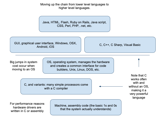
图 3.34 软件语言山。#
下一层是 C 语言代码。C 在这一级基本上占据了统治地位。过去还有 Pascal 等语言竞争,但如今几乎所有系统都有 C 编译器。C 设计于 Unix 诞生时期(这也解释了它为何成为苹果产品的基础)。C 和 C++ 之类的变体都使用编译器,它比汇编器更复杂。编译器在创建运行时文件时会做出决策,选择生成实际运行于 CPU 的机器码方式。需要知道的关键是,编译器虽能影响代码大小和执行速度,但它并不是语言到机器码的直接翻译。C 的一个强大特性是允许嵌入汇编代码,给你一种可以深入系统“内脏”的工具。C 已如此普及,最简单的微控制器都会有 C 编译器,让你能在无操作系统的系统中使用该语言(当然它也经常与操作系统一起使用)。
随着软件层级上升,反复出现的权衡是:开发速度和可移植性提升,但代价是更多系统资源消耗,包括 RAM、ROM 和处理能力。例如,你用某微控制器的汇编语言写了代码,但后来因某种原因要换 MCU。用汇编重新做工作非常耗时;若用 C 语言写,可以较快完成(相较于重写汇编版本),然后用新的编译器编译获得所需结果。用汇编能获得更高性能,但牺牲开发时间和可移植性。一般而言,若让我推荐今天最重要的编程语言,我会说是 C。[33] 一个原因是摩尔定律效应,随着密度增加,RAM、ROM 和 CPU 性能成本不断下降;自本书出版至今仅 6 年,中端 MCU 价格已下降 70–80%。这意味着你在很多情况下可以用高级的 C 语言编写代码而不必担心成本惩罚。即便成本更高,使用较小 MCU 的成本节约往往无法抵消使用汇编的开发成本。我知道这和之前那个电动牙刷控制器的例子有所不同,但世界在变,我们必须跟上。汇编依然有其地位,学习它仍有诸多好处。它肯定能帮助你理解机器的运作,并在你想充分利用机器让设备变得更出色时打下坚实基础。我也知道程序员通常更容易向上攀登软件阶梯,而不是从顶端向下。如果你想打造一个灵活的团队,就要有那些熟悉基础的人。一位工程师这样说:“向上过渡时,你要找到一个命令来完成你本来要写的 30 行代码(通常通过谷歌搜索实现),而向下过渡时,你需要知道如何写那 30 行代码。”
接下来是操作系统。它们不完全是编程语言,但在软件层次结构中非常重要。操作系统设计用来将代码编写者与硬件隔离。这样做的目的是为众多开发者创建统一的代码接口。操作系统管理硬件,处理 I/O、内存及其他系统资源,免去代码编写者的顾虑。但你可以写脚本和宏,由操作系统按需执行。操作系统通过驱动程序和 API [34] 与程序和系统硬件通信。驱动程序是较底层的,通常是 C 或汇编代码,用来控制某硬件,如 USB 端口。软件分层,需要在操作系统与程序层之间通信,这就是 API 的作用。
操作系统层之上是各种程序——其中改变世界的一类是浏览器。浏览器最初为联网程序创建统一界面,迅速成为电脑的主流。为了浏览器编程,更高级语言如 Java、PHP 等诞生。各种辅助编程的工具层出不穷。例如,Adobe Flash 帮助图形艺术家更方便地编写网页,但其视觉元素有限,Adobe 又推出了 ActionScript,这是一种更高级的编程语言。随着编程阶梯的攀升,语言对外行人变得更易读。[35] 一些高级语言被广泛使用,并衍生出“普通”编程的变体。例如,谷歌的 Android 是 Linux 上的 GUI 层,使用 Dalvik Java 虚拟机,让大量 Java 程序员能快速制作精美图形界面。
攀登软件山,你会发现速度和性能与设计的简易性、快速性及通用性之间总存在权衡。如果你能买得起更快的处理器,通常能更快推向市场,但讽刺的是,随着软件层层叠加,一年比一年厚,也为重写软件以提升速度和性能留出空间。谷歌 Chrome 就是例子;它是重新编写的浏览器,比以前更快更流畅。苹果的 OSX Snow Leopard 版本则通过剔除非必要层提升性能。
开发代码时,你不可避免会增加层级以避免重复编写代码,但到一定程度,系统就会变得臃肿。工程师或技术经理的诀窍在于找到因素间的最佳平衡——你需要理解产品成本、开发成本和上市速度成本,选出成功的最佳路径。
Awhile back I was explaining to my boss that software was written in layers; he looked at me and wondered why we would do that at all—seemed like a waste of time to him. Like extra work to have all those layers when it’s not needed. What I realized is that in today’s world SW (software) has become as ubiquitous as electricity itself; it is also as magical. Nowadays networks are common, and software is updated all the time. My phone, my computer, and even my treadmill are all getting software updates regularly. This has led to a complete misunderstanding by the layman of the complexity of software. To him or her it just takes care of itself. If we were making one product one time one layer of software would be sufficient, but the fact is that software is fundamentally integrated into more and more products in our everyday lives at an ever-increasing rate. To allow faster development, software engineers have created all sorts of tools. Now when I am speaking of software here, I am covering the full gambit of the term, including what we often call firmware, etc. —anything that executes lines of code. Building on this we will learn how and why software is layered and hopefully learn some more about general design and good practices when coding.
Take a look at Figure 3.34. At the bottom of the pile is the foundation, assem- bly or machine code. Machine code is the actual 1 and 0, true and false information that is processed in the CPU; assembly is one level slightly higher. I lump them together because not many write in machine code anymore. At the lowest level assembly is used; this is a set of mnemonics that represent the machine code, it which is turned into machine code by a piece of SW called an assembler. [32] It is a pretty direct translation from the mnemonic to the 1s and 0s the system can process.
FIGURE 3.34 Software language mountain.#
The next level up is C code. C has pretty much won out at this level. There were others like Pascal and such that competed, but there are very few systems today that do not have a C compiler. C was designed around the same time Unix came into being (that kind of explains why it is so foundational to Apple’ s pro- ducts). C and variants like C++ all use a compiler, which is something more complex than an assembler. A compiler makes decisions as it creates the run time file, choosing ways to create the machine code that actually runs on the CPU. The important aggregate thing to know is that while a compiler can affect the size of the code and the speed of execution, it is not a direct translation of the language written to the 1s and 0s. One very powerful aspect of C, though, is that you can slip in assembly code as you like when using it, giving you a tool that can reach down into the bowels of the system so to speak when you need it. C has become so ubiquitous that the most simple micros will have a C com- piler, giving you the ability to use that language in systems without an OS (note that it is often used with an OS as well).
There is one trade off as you move up the SW mountain that happens over and over. You get speed of development and portability but at a cost of using more system resources in terms of RAM and ROM and processing power. For example, you write a piece of code for one micro using their assembly language, but then you have to change out the MCU for some reason. To redo that work in assembly is very time consuming; however, if it is written in C you can go through it relatively quickly (compared to rewriting the assembly ver- sion, that is) and run the new compiler on it to get what you need. You will get more bang for your buck using assembly, but at the sacrifice of develop- ment time and portability. Now generally speaking, if I told someone today the most important language for them to learn, it would be C. [33] One reason for this is the effect of Moore’s law, the cost of RAM, ROM, and CPU power keep falling as densities increase; in just the 6 years since this book came out, the costs of midrange MCUs has fallen 70–80%. That means you can write in the higher level C language without suffering a cost penalty in many cases. Even if it costs more, the cost savings of using a smaller MCU often will not offset the development costs of using assembly. I realize this is a different take on things than in my toothbrush controller example from earlier, but the world changes and we have to keep up. Assembly still has its place, and I still think you will get many benefits learning it. It will certainly help you understand what the machine that you are working on is doing, and if you want to take full advan- tage of it to make whatever gadget you are building amazing, that foundation will always help. I also know that it is typically easier for a programmer to climb up the software ladder than it is for one to come down from the top. If you want to build a really flexible organization, get the types who know the foundation well. One of my EEs put it this way,“to transition up you have to find that one command that does the 30 lines of code you would have writ- ten (often accomplished by a Google search), but to transition down, you need to understand how to write those 30 lines of code.”
Next up we encounter operating systems. These aren’t exactly programming languages, but they are very important in the software mountain of layers. Oper- ating systems were designed to disconnect the code writers from the hardware they are working on. The reason for doing that was to make the code interface common for many, many, many different developers. An OS will manage the hardware, handle the I/O, memory, and other system resources so that the code writer doesn’t need to worry about it. You can, however, write script and macros that the OS will do as needed. Operating systems use things called drivers and APIs [34] to communicate with programs and with hardware in the system. Drivers are lower-level, typically C or assembly code that handle a piece of hardware, such as a USB port. Since software is layered, there needs to be a way to communicate between the layers from the OS to the programs; this is the job of an API.
On top of the OS layer are all sorts of programs—one type that changed the world was the browser. First invented to create a common interface for pro- grams connected on the Internet, it quickly became a mainstay of our compu- ters. To program for a browser, even higher level languages were created: Java, PHP, and so on. Programs to make programming easier are all over the place. For example, Adobe Flash is a tool that makes it easier for graphic artists to pro- gram web pages. However, still having limitations on the visual elements, Adobe created something called action script, which is yet an even higher level language for programming. As you move up the programming ladder you find that the language becomes more readable to the layperson. [35] Some of these higher level languages became widely used, and variations were created for “regular” programming. For example, Google’s Andriod is a GUI layer on Linux that is a Dalvik Java machine, which lets a huge crowd of Java programmers make slick graphic interfaces quickly.
As you climb up the software mountain you find that there are always trade-offs of speed and performance versus ease, quickness, and universality of design. If you can afford the faster processor, you can generally get to market faster, but ironically as this software mountain builds year after year, layer on layer, it opens up spaces for software to be rewritten to run better and faster. Google Chrome is an example of this; it is a browser recoded from the ground up to be quicker and faster than before. Apple’s OSX Snow Leopard release trimmed nonessential layers to improve performance.
As you develop code you invariably add layers to avoid rewriting sections of code, but at some point it becomes unwieldy for the system it is running on. The trick for an engineer or technical manager is knowing the right balance between the factors—you need to understand product costs, development costs, and speed to market costs to pick the best path for success.
拇指法则(Thumb rules)
汇编器通常是助记符到机器码的直接翻译。
高级语言占用更多系统资源,但一般更具可移植性且编程更快。
程序员向上攀登软件阶梯比向下更容易。
Assemblers are typically a direct translation from mnemonics to machine code.
Higher level languages use more system resources, but are generally more portable and quicker to program in.
Programmers can transition up the software ladder easier than down it.
输入与输出#
INPUT AND OUTPUT
这些设备的全部意义就在于输入一些信号以获得输出。因此,有必要花点篇幅讨论这个话题。
The whole point of these devices is to put something in just to get something out. So it stands to reason that it’s worthwhile to devote a few words to this topic.
输入#
Input
就像电影《短路》中的机器人一样,你设计的所有电路都需要输入。让我们回顾一些常见的输入设备及其相关信息。
有几种不同的方法可以将信号输入到你的 MCU 中。第一种方法是通过中断。你可以将信号接到一个能触发中断的引脚。当中断发生时,微控制器决定如何处理,然后继续执行。这种方式的优点是能立即获得微控制器的关注。
另一种监测输入线路的方法叫轮询。轮询的工作方式类似于那些讨厌的电话推销员 [36]。他们决定何时给你打电话询问信息。同样,微控制器决定何时检查某个引脚,并轮询该引脚获取信息。
第三种方式,即使是最小的微控制器也越来越常用,是进行模拟读取。按性质这是一种轮询操作,你需要告诉 A/D 何时进行读取。不过在某些情况下,可以将引脚设置为比较器,比较结果的输出可触发中断。基于此,我们来看看一些常见的输入设备。
Like the robot in the movie Short Circuit, all the circuits you will ever design will need input. Let’s review some common input devices and a little info about them.
There are a few different ways to get these signals into your MCU. One method is via an interrupt. You can hook a signal into a pin that can interrupt the micro. When it does, the micro decides what to do about it and moves on. This has the advantage of getting immediate attention from the micro.
Another way to monitor an input line is to use a method called polling. Polling works the same way those annoying telemarketers [36] do. They decide when to call you and ask for information. In the same way, the micro decides when to look at a pin and polls the pin for information.
A third way, becoming more and more common with even the smallest micro, is to take an analog reading. By nature this is a polling operation. You need to tell the A/D when to take a reading. In some cases, however, a pin can be set up as a comparator, and the output of that comparison can drive an interrupt. With that in mind, let’s take a look at some common input devices.
开关#
SWITCHES
你最可能遇到的最基础的输入设备是开关。开关闭合时呈低阻抗,断开时则表现为理想的高阻抗连接。因为断开时开关是断开的,闭合时几乎相当于完美短路。这一点很重要,因为如果你将开关接到 MCU 的高阻抗端口,开关断开时你将得到高阻抗 [37] 对高阻抗连接,这很可能导致一些奇怪的结果。阻抗越高,信号越容易受干扰。为了解决这个问题,使用上拉或下拉电阻。
上拉(或下拉)电阻用于确保当没有其他动作时,输入线路有一个已知状态,如 Figure 3.35 所示。如果你的开关按下时将线路接地或接参考电压,则使用上拉电阻将信号“拉”到 Vcc。相反情况则使用下拉电阻 [38] ,如 Figure 3.36 所示。
图 3.35 带上拉电阻的开关。#
图 3.36 带下拉电阻的开关。#
一般来说,轮询开关输入比让其触发中断更好。这是因为开关抖动现象。开关作为机械装置,内部有两点接触。当它闭合时,接触点可能会在最终闭合前反复开合几次。接点实际上会弹跳几下。微控制器收到的输入信号如 Figure 3.37 所示。
图 3.37 开关弹跳时信号线的情况。#
如果系统是中断驱动的,你可以想象会发生什么。每当信号变高,微控制器都会触发一次中断。而你其实只想要开关闭合时发生一次动作,结果可能触发五六次中断。如果你对该线路进行轮询,可以通过检查频率低于弹跳频率来忽略这个问题。[39] 另一种增强鲁棒性的方法是要求连续两次轮询信号都检测为闭合,才认为开关闭合。这样能有效避免故障或噪声被误判为有效输入。
Probably the most basic input device you will encounter is the switch. A switch is a low-impedance device when it is closed and the perfect high-impedance connection when it is open. This is because an open switch is disconnected and a closed switch is about as close as you can get to a perfect short. This is important to note because if you are connecting a switch to a high-impedance port on your MCU, when it is open you will have a high impedance [37] connected to a high impedance. This is a sure way to get some weird results. The higher the impedance, the more easily disrupted the signal. To combat this, use a pull-up or pull-down resistor.
A pull-up (or -down) resistor is used to make sure that when nothing else is going on you get a known state on your input line, as shown in Figure 3.35. If you have a switch that, when pressed, connects the line to ground or reference, use a pull-up resistor to“pull” the signal “up” to Vcc. For the opposite situation, use a pull-down resistor, [38] as shown in Figure 3.36 Figure 3.36>.
FIGURE 3.35 Switch with pull-up.#
FIGURE 3.36 Switch with pull-down.#
Generally it is better to poll a switch input than to let it trigger an interrupt. This is due to a phenomenon called switch bounce. Being mechanical in nature, a switch internally has two points that come in contact with each other. As they close, it is possible for them to bang open and shut a few times before they close all the way. The contact actually bounces a few times. The input signal to the micro looks like the diagram in Figure 3.37.
FIGURE 3.37 What happens on a signal line when a switch bounces.#
If this is an interrupt-driven system, you can see what might happen. Every time the signal goes high, an interrupt is tripped in the micro. When you really only wanted a single action to occur from the switch closing, you might get five or six trips of the interrupt. If you poll this line, you can determine the frequency of the bounce and essentially overlook this problem by check- ing less often than the frequency of the bounce. [39] Another way to add some robustness is to require two polled signals in a row before you consider the switch closed. This will make it difficult for glitches or noise to be considered a valid input.
晶体管#
TRANSISTORS
由于晶体管的普遍使用,你很可能在某个时候需要将其作为输入设备进行接口。像开关一样,晶体管在导通时为低阻抗,关断时为高阻抗,因此需要使用上拉或下拉电阻。你需要使用哪种电阻取决于所读取的晶体管类型。(参见本章开头。)一般来说,NPN型晶体管需要上拉电阻,PNP型则需要下拉电阻。
Because of the ubiquitous usage of the transistor, it is likely that you will need to interface to it as an input device at some time or another. Like the switch, the transistor is low impedance when it is on and high impedance when it is off, necessitating the need for a pull-up or pull-down resistor. Which one you need depends on the type of transistor you are reading. (See the beginning of this chapter.) Generally you want a pull-up for an NPN type and a pull-down for a PNP type.
光敏晶体管#
PHOTOTRANSISTORS
光敏晶体管是晶体管的一个近亲。它是一种对光敏感的晶体管,常用于检测某种运动,例如电机轴上的编码器。
你应将其视作普通晶体管来处理。但请注意,光敏晶体管的增益或β值变化范围远大于普通晶体管。设计时需要考虑这一点。还应检查这些晶体管的电流能力。通常它们无法吸收像普通晶体管那样大的电流,因此不要给它们施加过大负载。
A cousin to the transistor is the phototransistor. This is a transistor that responds to light, often used to detect some type of movement, such as an encoder on the shaft of a motor.
You should treat it the same way as a regular transistor. Note, though, that phototransistors have a gain or beta that can vary much more than a regular transistor. You will need to account for that in your design. Another thing you should check with these transistors is their current capability. Usually they won’t sink nearly as much current as the basic plain old transistor will, so don’t put too much of a load on them.
霍尔传感器或磁传感器#
HALL OR MAGNETIC SENSORS
霍尔传感器或磁传感器是能感应磁场存在的器件。它们种类繁多,从称为簧片开关的小金属片(靠近磁铁时闭合)到能输出模拟或数字信号的集成电路均有。你需要查看这些器件的输出规格以决定如何设置。例如,簧片开关可以当作开关处理(是的,它也会“弹跳”),而霍尔器件可能带有晶体管输出,设置方式则不同。
Hall or magnetic sensors are devices that can sense the presence of a magnetic field. They come in all types and flavors, from items called reed switches (little pieces of metal in a tube that close when near a magnet) to ICs that can output an analog or digital signal. You will need to look at the output specs on these parts to determine how to set them up. For example, the reed switch you treat like a switch (yes, it can“bounce,” too) whereas the hall device might have a transistor output and need a different setup.
数字编码器#
DIGITAL ENCODERS
数字编码器是开关的近亲,旋转旋钮时会切换线路。像开关一样,需要上拉或下拉电阻以确保读取可靠。
A cousin to the switch, a digital encoder switches lines together as you rotate the knob. Like the switch, you will need pull-up or pull-down resistors to ensure reliable readings.
其他集成电路#
OTHER ICs
还有许多其他芯片可以提供信号。与其他芯片通信时,时序非常重要。通常你通过输出信号激活目标芯片,然后读取返回的数据。内存芯片就是例子:你在地址引脚上输入地址,再从数据引脚获取数据。你需要考虑芯片响应命令所需的时间。每个数字芯片都有响应时间或传播延迟,你必须确保等待足够长时间后再读取信号。如果你与目标芯片之间有多个芯片,还需将这些延迟累加考虑。不要简单地组装好后直接测试,这样很可能造成看似随机、难以解释的故障,因为有的芯片速度比规格更快,实验室样品没问题,但批量生产时就出现问题。
There are a multitude of other chips out there from which you can get signals. One thing that is important when talking to other chips is timing. Often you activate the chip you are talking to with an output signal, and then you look at the data coming back. A memory chip is an example of this. You present the address on the address pins and then grab the data from the data pins. One thing you need to consider is the time it takes for the chip to respond to this command. Every digital IC has a response time or propagation delay for it to respond to a signal. You need to make sure you wait long enough for the signal to be present before you try to get it. If there is more than one IC between you and the chip you are talking to, you need to add those delays in as well. Don’t just put it together and see if it works without checking this out. It is not uncommon for a chip to be faster than the spec, so one in the lab might work fine, yet when you get into production you will see a seemingly random failure that defies explanation.
输入规格#
INPUT SPECS
在进入模拟输入之前,数字输入有一项重要事项需知。每个微控制器都有输入规格,称为阈值。这是信号被认为为高电平或低电平所需达到的最小和最大电压。你必须确保信号超过最大阈值或低于最小阈值。如果信号在两者之间,即使表面看似正常,也会给你带来后续麻烦。请记住,在这两个值之间,微控制器无法确定信号是高还是低,它会将信号解析为其中之一,但你无法确定是哪一个。
Before we move on to analog inputs, there is an important thing to consider when we’re dealing with digital inputs. Every micro has input specifications known as thresholds. These are the minimum and maximum voltages a signal must reach to be considered a high or a low. You need to make sure that your signal gets above the maximum and below the minimum. If it spends any time in between, even if it seems to be working right, you can be sure it will cause you trouble down the road. Just remember, between those two values you can’t be sure what the micro will consider the signal to be. You won’t know if it is a high or low; the micro will resolve it as one or the other. You just can’t be sure which one.
电位器#
POTENTIOMETERS
电位器(也称为电位计)是一种带有三个端子的可变电阻,通常称为高端、滑动端和低端。在高端和低端之间测量会得到一个电阻值。滑动端是一个可动连接点,会接触上述电阻的不同位置。图 3.38 显示了其示意图。
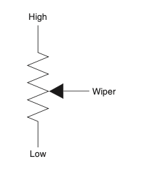
图 3.38 电位器示意图。#
如果你将输入电压接到高端,滑动端接输出,低端接地,那么你得到的就是前面学习过的分压器。电位器的便利之处在于,转动旋钮即可轻松调节这个分压器。如 图 3.39 所示,将滑动端接到任一端,你就创建了一个随旋钮转动而变化的可变电阻。电位器用途广泛——用于调整电路中的值(甚至是没有微控制器的电路,信不信由你!)、调试设备至正确工作状态等。涉及 MCU 时,你可能会用它作为项目中调节数值的便捷方式。通常通过 A/D 输入读取其值。
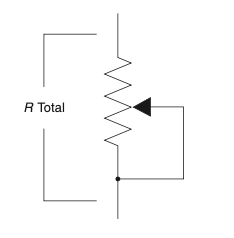
图 3.39 由电位器构成的可变电阻。#
一般来说,电位器的阻值公差较大,可能高低端相差 ±20%。但若用作分压器,这种差异会被显著抵消。因为整体电阻变化时,滑动端某个位置所占电阻比例变化并不大。
Potentiometers (also called pots) are a type of variable resistor with three connec- tions, commonly called high, wiper, and low. Measuring between pins high and low, you will see a resistor. The wiper is a connection that as it moves touches the aforementioned resistor at various locations. Figure 3.38 shows a diagram of one.
FIGURE 3.38 Diagram of a potentio-meter.#
If you hook the input voltage to high, wiper to the output, and low to ground, you have nothing more than the voltage divider that we learned about earlier. What is more convenient about the pot is that this voltage divider is easily adjustable by the turn of a knob. If you tie the wiper to one end or the other as shown in Figure 3.39, you will have created a variable resistor that changes as you move the knob. These are used in myriad ways—to adjust values in a circuit (one without a micro, if you can believe it!) or to tune a device into the correct operation and many other cool things. As it relates to an MCU you might find yourself hooking one of these up as a slick way to dial a value on your project. Commonly you will read these with an A/D input.
FIGURE 3.39 Potentiometer made into a variable resistor.#
Generally, pots have a large tolerance, changing by as much as ±20% in resis- tance, high to low. However, if used in a voltage divider configuration, this var- iance is canceled out considerably. This is because, while the overall resistance changes, the percentage of resistance for a given position of the wiper doesn’t vary nearly as much.
模拟传感器#
Analog Sensors
热电偶、光电二极管、压力传感器、应变计和麦克风只是众多模拟传感器中的几种。传感器种类繁多,不可能全部涵盖,但这里给出一些使用各种传感器的良好指导原则。
Thermal couples, photodiodes, pressure sensors, strain gauges, and micro- phones are just a few of the plethora of analog sensors available. There are so many options that there is no way to cover them all, but here are some good guidelines for using various sensors.
接地#
Grounding
传感器的接地线应该接到哪里?处理模拟传感器时,必须关注传感器的接地线以及电源线。信号线通常直接回到读取它的芯片,但接地或电源线可能会经过多个集成电路(IC)后才连接到读取信号的芯片相应引脚。这会导致来自其他IC的电流干扰传感器信号电流。如果你的传感器检测的是微弱信号,比如应变计,这种干扰可能会很糟糕。
不良情况:来自IC的接地电流在传感器信号上产生噪声——见 图 3.40。良好做法:走线回到芯片,保持模数转换器(A/D)参考点与A/D输入处于同一位置,如 图 3.41 所示。
图 3.40 不良的模拟地布线布局。#
图 3.41 优化后的模拟地布线布局。#
Where does the sensor ground go? Dealing with analog sensors requires pay- ing attention to the ground as well as the power source for the sensor. Often the signal line will come right back to the chip reading it, but the ground or power leg might run past multiple ICs before getting to the corresponding pin on the chip reading the signal. This allows currents from all those other ICs to interfere with the current from the sensor. If your sensor is looking at some small signals such as a strain gauge or the like, this can be a bad thing.
Bad: Ground currents from ICs cause noise on the sensor signal—see Figure 3.40. Good: Traces go back to the chip, keeping the A/D reference where the A/D input is, as shown in Figure 3.41.
FIGURE 3.40 Poor analog ground layout.#
FIGURE 3.41 Much better analog ground layout.#
传感器阻抗#
Sensor Impedance
你的传感器输出阻抗是多少?如果相对于所连接的负载[40]_太高,可能导致信号不能按预期变化。你可能需要缓冲器来避免负载影响传感器。
What is the output impedance of your sensor? If this is too high with respect to the load [40] it is hooked up to, it might not change the signal in the way you expect. You might need to buffer the sensor so that it is not affected by loading.
输入阻抗#
Input Impedance
大多数A/D转换器有一定输入阻抗,通常远低于数字输入。数字输入阻抗通常为5MΩ至10MΩ,而A/D输入大约为100KΩ。你应了解你的输入阻抗,并确保其明显高于传感器输出阻抗,避免影响信号。100:1的阻抗比是一个良好起点。例如,A/D输入为100KΩ,传感器输出低于1KΩ,最大误差约1%;若设计允许,则可接受。
Most A/D converters have some type of input impedance, usually significantly lower than a digital input. A digital input is often 5 to 10 M ohms of impedance, whereas an A/D may be 100 K ohms. Get to know your input impedance, and make sure it is adequately higher than the sensor output impedance so that it’s not an issue. A ratio of at least 100:1 is a good place to start. That means that if your A/D is 100 K and your sensor has less than 1 K output impedance, you will have a maximum error of 1%; if that is acceptable in your design you are probably okay.
输出#
Output
你可以将信号输出到多种设备,这里介绍几种常见的指示器和显示器。现今最常见的是LED和LCD。
There are numerous devices that you can output a signal to. We will cover a few of them here. Let’s start with some common indicators and displays. Two that are the most common these days are the LED and the LCD.
LED#
LEDs
LED意为发光二极管。LED需要电流驱动。电流太小不会发光,太大则会损坏,通常需串联限流电阻。所需电流取决于LED类型,20mA是常见工作电流。LED是电流驱动器件,其亮度取决于通过的电流(而非两端电压)。这也意味着可以通过改变串联电阻调节亮度(见 图 3.42)。
用微控制器驱动LED时,需要考虑芯片的输出能力。输出引脚能提供足够电流吗?能承受电流流入吗?许多微控制器能承受电流流入引脚,但不能输出电流。因此,我通常采用将LED接地驱动方式——见 图 3.43。
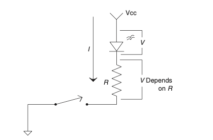
图 3.42 开关控制的LED电路。#
图 3.43 MCU控制的二极管。#
你看到了电流流入微控制器吗?必须确保输出引脚能承受此电流!且电流从MCU地线引脚流出回到电源。
LED有一个压降,就像我们之前学习的二极管一样。新的蓝色和白色LED压降比我小时候常见的红色、绿色、黄色LED高得多。红绿黄LED压降约1.0至1.5伏,蓝色LED可达3.5伏。
图 3.44 显示了如果你的MCU电源只有3.3伏,你可能考虑用此方式驱动蓝色LED。但我不推荐,因为存在潜在问题。你看出来了吗?
该电路的问题出现在使用成本较低、较老的红/黄/绿LED时。因压降较小,若输出引脚为3.3伏,而LED另一端接5伏,则电阻和二极管上可能有1.7伏,足以让LED弱亮。
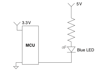
图 3.44 用3.3伏MCU控制3.5伏LED的较弱方案。#
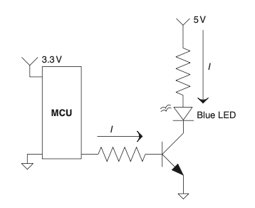
图 3.45 用3.3伏MCU更稳健控制3.5伏LED的方案。#
图 3.45 显示了同样条件下更好的蓝色LED驱动方法。LED驱动的教训是:务必关注通过LED所需的压降,以保证电流正常流动。
好了,够了那些闪烁的灯光;我们来看看更“流动”的东西。
LED stands for light-emitting diode. LEDs need current to drive them. Too little and you won’t get any light, too much and they will fail, so you typically need a series resistor. How much current is needed depends on the type of LED, but 20 mA is a common normal operating current. LEDs are current-driven devices; this means that their brightness depends on the amount of current flowing through them (not the voltage drop across them). This also means that you can control the brightness by changing the series resistor (Figure 3.42). An important thing you should consider when driving an LED with a micro is the output capability of the chip. Does the output pin have the ability to source enough current? Can it sink enough current? There are plenty of micros out there that can sink current into a pin but can’t source it. For this reason I will typically drive an LED by sinking it—see Figure 3.43.
FIGURE 3.42 Switch-controlled LED circuit.#
FIGURE 3.43 Diode controlled by MCU.#
Do you see how the current flows into the micro? You need to make sure the output pin can handle it! Also, take note that the current flows out of the ground pin on the micro and back to the source.
LEDs have a voltage drop across them, just like the diode that we have already learned about. The new cool blue and white ones are quite a bit higher than the ones I was raised on. Red, green, and yellow LEDs are around 1.0 to 1.5 V, whereas the blues can easily be 3.5 V.
Figure 3.44 shows a way that you might consider driving one if your MCU has only 3.3 V available as a supply. I wouldn’t recommend it, though, because it has a potential problem. Do you see what it is?
The problem with this circuit comes when you try to use the less-expensive, older red/yellow/green diodes. With a smaller voltage drop, current might still flow if the output pin is at a high of 3.3 V and the other end of that diode is at 5 V. Do the math: That would leave 1.7 V across the resistor and the diode, enough to turn it on, albeit weakly in most cases.
FIGURE 3.44 Less robust way to control a 3.5-V LED with a 3.3-V MCU.#
FIGURE 3.45 More robust way to control a 3.5-V LED with a 3.3-V MCU.#
Figure 3.45 shows a better way to drive a blue LED under the same constraints. The moral of the LED story is pay attention to the voltage drop needed to get current moving through it.
Well, enough of the pretty blinky lights; let’s examine something that is more fluid.
液晶显示器#
LCDs
LCD代表液晶显示器。液晶是一种对电场有响应的材料——见 图 3.46。对液晶两侧施加电场,会使液晶分子沿某一方向排列。如果足够多的液晶分子排列整齐,光线将被阻挡,无法透过。
如果对LCD施加偏压时间过长,液晶将永久扭曲,且无法恢复。就像你长时间盯着电脑屏幕导致脖子僵硬一样。如果不时起身活动,你的状态会好转。液晶也是同理,必须不时反转偏压极性,让所有液晶分子反向排列。它们仍阻挡光线,但方向相反。
这使得驱动LCD略显复杂,因为你必须不断切换极性。多路复用LCD时更复杂,你必须确保某段区域不会长时间承受直流偏压等等。[41]
图 3.46 LCD内部结构。#
因此存在LCD驱动芯片。有时此功能集成在微控制器中,另一些情况需单独芯片。你可以自己设计驱动,但我不推荐,容易出错且驱动芯片价格低廉。
由于液晶响应电场,驱动LCD类似于驱动电容。每次切换LCD时都会消耗少量电流。记得RC电路吗?电流很小——相较于LED,几乎可以忽略不计。电流低到手表显示可以用电池维持多年。但注意,段越大,电容越大,[42] 需要更多电流。
LCD stands for liquid crystal display. The liquid crystal in an LCD is a material that responds to an electric field—see Figure 3.46. Applying an electric field to either side of the crystal will make the crystal molecules line up in a certain direction. If you get enough of these crystals lined up, light will be blocked from passing through it.
If you leave an LCD biased for too long, the liquid crystal will permanently twist and you won’t be able to twist it back. It is like the crick in your neck that you get from sitting in front of the computer too long. If you don’t get up and move a bit every so often, you will tend to stay that way. Though that’s good entertainment for fellow employees, a little motion will save you the pain.
The same philosophy works with LCDs. Every so often, reverse the polarity on the LCD and all the crystals will swap direction. They still block the light, but they are all pointing the other way.
This makes driving an LCD a bit high maintenance, since you have to keep coming back to it to tell it to swap things up. It gets even more complex when you begin to multiplex the LCDs, too. You need to make sure you don’t leave a cumulative DC bias on one of the segments too long, etc. [41]
FIGURE 3.46 Inside an LCD.#
For this reason, there are LCD driver chips. Sometimes this feature is built right into the micro; in other cases, it will require a separate chip. You can go it alone and make your own driver, but I don’t recommend it. It is easy to mess this up, and LCD drivers are pretty cheap.
Since it is an electric field that changes the LCD, driving the LCD is a bit like driving a capacitor. Every time you switch the LCD, a little current is used. Remember the RC circuit? It is not much—in comparison to LEDs, it is virtually insignificant. You can get the current so low that a watch display can last for years on a battery. Remember, though, the larger the segment, the larger the cap, [42] and this means more current is needed to run the LCD.
多路复用#
Multiplexing
如何同时做多件事?实际上你做的是快速地一件一件处理,使得看起来像多任务。(就像一边看电视一边听配偶说话,适时点头效果奇佳。)
图 3.47 LED多路复用示意。#
电气工程师中,多路复用十分实用。即用更少输入控制更多输出。看 图 3.47,你可以通过引脚1拉低、引脚2拉高让电流流过L1和L2。
由于LED的单向导电性质(类似单向阀),引脚1为低时,引脚A或B为高则点亮相应LED。交换引脚1和2,则点亮L3和L4。重复切换速度足够快时,人眼看见的LED是持续亮的。例中四个引脚控制四个LED,仅为示例;增加每组LED数量,能控制的LED数迅速增多。三灯一组时,用5个引脚控6灯;四灯组时6个引脚控8灯,依此类推。两组八灯时10线控16灯!这在I/O资源有限的项目中尤为方便,尤其当项目负责人拒绝你用带更多I/O的更贵微控制器时。注意,此方法依赖二极管只能单向导电。
How do you do more than one thing at a time? Actually, you don’t—you do several things quickly one at a time so that it appears that you are multitasking. (Like listening to your spouse while you are watching TV. A timely nod of the head can do wonders.)
FIGURE 3.47 Multiplexing LEDs.#
In the world of sparkies, it can be useful to multitask. One way to do this is by the art of multiplexing, that is, using fewer inputs to drive more outputs. Take a look at the example in Figure 3.47. In this case you can enable current to go through L1 and L2 by putting a low signal on pin 1 and a high signal on pin 2.
Due to the diode nature of the LED (think one-way valve) with a low on pin 1, putting a high on pin A or B will illuminate the appropriate LED. Reversing pins 1 and 2 will enable L3 and L4 to be illuminated. Repeat this process fast enough and to the human eye the LED will appear to be continuously lit. In this example we use four pins to talk to four LEDs, just to keep things simple, but increase the number of LEDs in each bank and you will quickly see how fast the number of LEDs you can talk to increases compared to the pins used. With three LEDs per bank, you have five pins running six lights; with four you have six pins running eight lights, and so on. If you have two banks of eight, you will have 10 lines controlling 16 LEDs! That is handy, especially when I/O is critical on that project where the PHB told you no, you can’t have that more expensive micro with all the extra I/O. Remember, though, this application relies on the fact that the diodes pass current in only one direction.
白炽灯#
Incandescent
另一种指示器是白炽灯泡,基本就是灯泡。真空管内的电阻丝加热到发光。加热耗电量大,微控制器引脚很少能直接驱动灯泡。
Another indicator, the incandescent bulb, is basically a light bulb. A resistive element in a vacuum tube heats up so much it gives off light. The fact that it heats up so much should trigger the light bulb over your head, so you are saying to yourself,“I bet that it uses a lot of current!” Which it does; it is rare that a micro has enough current capability to drive a lamp directly from a port pin.
晶体管和场效应管#
Transistors and FETs
双极晶体管(BJT)或场效应管(FET)是改变电压或提升微控制器输出电流能力的好方法(如蓝色LED电路所示)。用BJT时别忘了串联基极电阻,限制电流,因你是在开关一个接地二极管。FET则需防过压或静电击穿。
A bipolar junction transistor (BJT) or an FET is a great way to change the voltage (as we saw with the blue LED circuit) or to step up the output current capability of a micro. Don’t forget to use a series resistor to the base with the BJT; you need to limit the current as you are switching a diode to ground. With the FET, protect the device from overvoltage or static shocks.
线圈#
Coils
许多设备含线圈或电感器,你可以向其发送信号。例如继电器。可能能直接驱动,但先检查电流需求!通常需用晶体管驱动。同时需要并联反向二极管防止电感反冲电压损坏元件。详细内容请见 第4章 “捕捉飞虫”部分。
All sorts of devices have coils or inductors in them that you can send signals to. Let’s take relays, for example. You might be able to drive them directly, but check the current requirements first! You will often need to use a transistor to handle the load. Also, you will need a reverse-biased diode in parallel with the coil (to prevent excessive voltage spikes from causing damage). You can look at the section“Catching Flies” in Chapter 4 to learn more about the inductive kick on a coil and what to do about it.
经验法则(Thumb Rules)
输入设备高阻时,使用上拉或下拉电阻确保输入信号有效。
中断驱动输入会暂停微控制器当前任务,响应输入。
轮询输入允许你自控读取时间。
输入设备种类繁多,设备数据手册非常重要。
可多路复用LED,节省I/O口。
晶体管是改变电压等级的利器。
设备中含线圈或电感需特别注意。
Use pull-up or pull-down resistors to assert an input signal when the input device is high impedance.
Interrupt-driven inputs stop whatever the micro is doing while the line is active.
Polling inputs allow you to control when you want to look at the inputs.
Input devices come in an infinite variety of packages and capabilities, making the datasheet on the device very important.
You can multiplex LEDs to scare up some needed I/O.
Transistors are a great way to change voltage levels.
Watch out for coils or inductors in devices; they will need some special consideration.